Inrush Current Limiter with NCP45560
Nov 1,2025
Preface

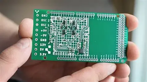
aims to resonate with engineers by depicting common debugging dilemmas, visually introducing inrush current as the "culprit," and setting the stage for introducing the NCP45560 solution.
Every engineer remembers that one prototype that powered up just fine—until it didn’t.
No smoke, no drama, just a flicker of LEDs, a reset that made no sense, or that faint spark at the connector.
Those small clues point to one culprit: inrush current, the burst of charge every capacitor demands the instant voltage appears.
In dense boards—routers, LoRa gateways, or RF modules—the first milliseconds decide whether the supply rail stays solid or dips low enough to confuse your logic section.
That invisible surge can trip UVLO in upstream converters, scramble PG signals, or even wear connectors over time.
Taming it means shaping how your power rail wakes up.
That’s where a controlled-start device like the onsemi NCP45560IMNTWG-H, part of the ecoSWITCH™ line, makes a real difference.
Instead of brute-forcing with resistors or thermistors, it gives your 5 V or 12 V line a smooth, predictable slope—soft-starting the system rather than shocking it awake.
When Does Inrush Actually Threaten Your 5 V / 12 V Rail?
At first glance, the math seems harmless.
A single 470 µF bulk capacitor behind a 12 V jack looks ordinary—until you realize it can gulp over 10 A in the first microseconds.
That’s enough to drag your main rail down, glitch the MCU, or trigger a UVLO reset in your DC/DC converter.
Real boards tell the story better than equations:
- Microcontrollers reboot the moment power plugs in.
- The PGOOD line jitters instead of asserting cleanly.
- You hear a soft pop when connecting the barrel jack.
- RF amplifiers drop out mid-transmit even though supply current seems fine.
You’ll see these quirks in communication gear, fan controllers, and mixed-signal boards with large local capacitance.
The physics are simple—I = C × dV/dt—but the fix isn’t just math; it’s about pacing.
Slow the rise a little, and the chaos disappears.
For related power-path behavior, TEJTE’s RF Coaxial Cable Guide discusses how voltage transients also affect signal return paths—useful context when power and RF share ground planes.
Should You Use an NTC, an eFuse, or a High Side Switch for Inrush?
There are three classic tricks, and each has its quirks.
NTC thermistors are the first tool many engineers grab.
They’re cheap and self-regulating—but also unpredictable.
When cold, resistance is high and limits the surge; once they heat up, it drops, leaving almost no damping.
On DC rails that toggle frequently, every re-plug starts “cold,” bringing that resistance spike right back.
A fixed resistor behaves the same every time, which sounds nice until you realize it wastes voltage all the time.
At 3 A, even 0.5 Ω burns 4.5 W—hardly elegant in a compact board.
Then there’s the eFuse, a smart IC that measures and enforces current limits with retry logic and telemetry.
They’re robust but complicated.
When you simply want to soften the voltage ramp, the overhead can feel like using a sledgehammer to crack an egg.
Enter the middle ground: a high-side load switch with controlled slew rate, like the NCP45560IMNTWG-H.
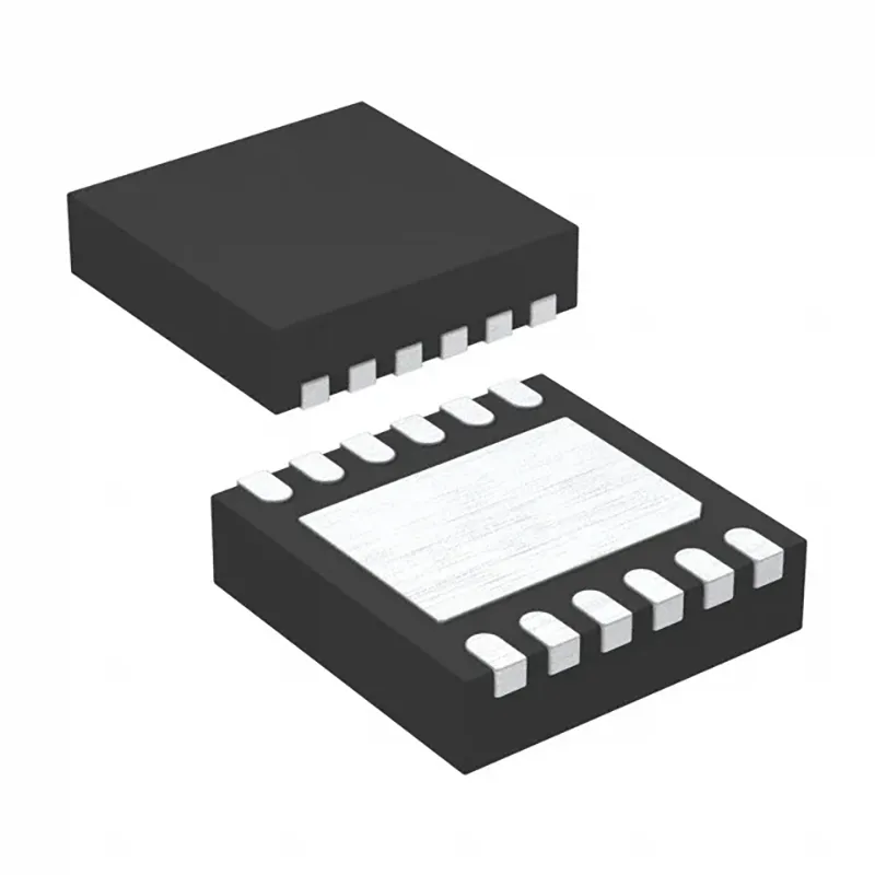
This device uses a precision-driven N-channel FET—rated up to 17 A output with 3.2 mΩ typical R_DS(on)—to shape the voltage rise automatically.
It integrates PGOOD, UVLO, and thermal protection (OTP), cutting external parts to nearly zero.
With a 0.5 – 13.5 V load range and 3 – 5.5 V logic supply, it fits right into the 5 V and 12 V ecosystems most engineers work with daily.
Choosing between these isn’t about which chip looks smarter—it’s about how predictable your startup needs to be.
If you value simplicity and consistent timing, a slew-limited high side switch usually wins.
For advanced power routing and layout practices, see TEJTE’s MOSFET Guide which touches on low-R_DS(on) design and thermal spreading.
How Does NCP45560’s Slew-Rate Control Limit I = C·dV/dt Safely?
Let’s anchor the theory in numbers.
Suppose the 12 V rail must charge 470 µF of capacitance within 2 ms.
By I = C·V/t, inrush current ≈ 2.82 A.
That’s well below the device’s 17 A peak capability, leaving generous thermal room.
Inside the chip, a feedback-regulated driver adjusts the FET’s gate charge rate, enforcing a clean slope rather than an abrupt turn-on.
When output voltage reaches its valid window, the PGOOD flag goes high, signaling downstream converters or RF PAs that it’s safe to start.
If Vcc < 3 V, UVLO holds the switch off; if the junction rises above 125 °C, OTP intervenes.
Steady-state power loss stays tiny.
At 5 A, P = I² × R_DS(on) = 25 × 0.0032 ≈ 0.08 W, comfortably handled by the 12-DFN (3 × 3 mm) package when copper and vias are adequate.
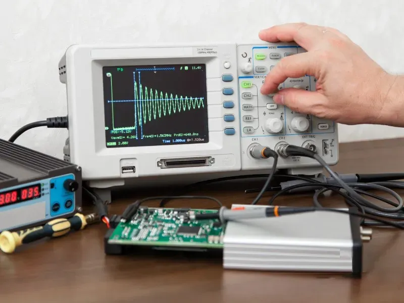
On the bench, the change is easy to see—scope traces that used to spike now glide upward, and the supply sounds silent when plugged.
That smoothness isn’t just aesthetic; it means less EMI, fewer retries, and longer connector life.
You can find related surge-control insights in TEJTE’s TVS Diode Selection Guide, which complements the same idea of graceful energy absorption rather than brute suppression.
How Slow Should the Slew Be to Stay Safe?
The safest way to manage inrush current isn’t guessing—it’s measuring.
Too fast, and the capacitors drag the rail down.
Too slow, and startup feels lazy or conflicts with other rails.
The trick lies in controlling slew rate, matching the capacitor load, and respecting your switch’s thermal limit.
To simplify, the current during ramp-up follows:
[ I_\text{inrush} = C_\text{load} \times \frac{V_\text{rail}}{t_r} ]
and the instantaneous power dissipated inside the high side switch is:
[ P_\text{inst} ≈ I_\text{inrush}^2 × R_{DS(on)} ]
With NCP45560IMNTWG-H, rated 3.2 mΩ typical and 17 A peak, you can estimate both thermal and timing margins.
Below is a simple reference card for quick validation:
| Input | Typical Value | Formula / Result | Interpretation |
|---|---|---|---|
| V_rail | 12 V | — | System voltage |
| C_load | 470 μF | — | Bulk capacitor |
| Rise time (t_r) | 2 ms | I_inrush = 2.82 A | Surge current peak |
| R_DS(on) | 3.2 mΩ | P_inst = 0.025 W | Initial heating load |
| E_pulse | ≈ 0.05 mJ | ∫P dt (triangular model) | Transient thermal energy |
A result within 20–30 % of steady-state thermal rating typically passes safely.
If it fails, you have three choices:
- Increase t_r (slower ramp).
- Split rails—charge bulk caps in stages.
- Upgrade to an eFuse if precise short-circuit protection is mandatory.
On PCB level, spreading heat through vias under the DFN-3×3 package dramatically improves pulse tolerance.
onsemi’s datasheet recommends at least 5–6 thermal vias beneath the pad to spread heat across inner planes.
For layout tips on how copper thickness and via count affect real current handling, TEJTE’s Low R_DS(on) Layout & Thermal Guide has detailed copper-area case studies from real PCB builds.
How to Wire PGOOD for Clean Sequencing with Downstream Rails
Once your inrush current limiter tames the surge, sequencing becomes the next challenge.
In multi-rail systems—say, 5 V digital + 12 V RF path—turning things on in the wrong order can trigger half-logic states or brown-outs.
The NCP45560 integrates a PGOOD output that asserts only when the load voltage crosses the internal threshold.
You can route this signal to the EN pin of the downstream DC/DC converter or RF PA enable line, effectively chaining the sequence:
“Main rail first → load stable → sub-regulators enable.”
That single connection avoids the “power-good bounce” that often plagues RF front-ends when their enable lines float early.
During shutdown, the same path works in reverse: disable the PA first, then let the main rail fall naturally.
Good sequencing reduces stress on components, ensures predictable RF calibration, and prevents DC/DC converters from latching into current-limit mode at boot.
It’s a subtle but powerful use of a simple digital flag.
You can find practical PGOOD timing and signal-handling discussions in TEJTE’s RF Antenna Integration Guide, which explores how consistent supply sequencing improves RF front-end reliability.
What PCB Layout Practices Keep R_DS(on) and Heating in Check?

corresponds to the "What PCB Layout Practices Keep R_DS(on) and Heating in Check?" section. It visualizes the textual layout guidelines (e.g., using 5-6 thermal vias) and is a key reference for ensuring high-current performance.
Even the best power distribution switch can underperform if layout is careless.
At double-digit amps, millimeters of copper trace start behaving like resistors.
The NCP45560’s DFN-3×3 package needs short, wide traces—ideally less than 1 mm between VIN and VOUT pins—and a continuous ground return plane.
Here are the essentials from field experience:
- Place input and output capacitors within a centimeter of the switch pins.
- Use thermal vias directly under the exposed pad—tie them to inner and bottom copper.
- Avoid routing sense or control traces under high-current paths.
- Keep PGOOD and EN lines away from switching nodes to prevent jitter or false detection.
When verifying thermals, it helps to measure surface temperature after 5 minutes at nominal load.
If you’re under 60 °C rise, the copper and via network are doing their job.
If not, consider doubling plane width or spreading heat toward the connector area.
A common mistake is isolating the copper pad electrically for fear of shorts.
In reality, tying the exposed pad to system ground improves both EMI stability and thermal headroom.
That’s particularly important in RF-linked systems, where impedance consistency matters as much as thermal design.
For real assembly guidelines—stencil aperture, via fill, and solder pad geometry—see the DFN mounting section in onsemi’s application notes or TEJTE’s own Connector Layout Standards, which share similar footprint principles.
What Protections & Monitors Remain Necessary Around the Switch

Even with a well-tuned inrush current limiter, no single IC can do every job on its own.
The NCP45560IMNTWG-H includes UVLO, PGOOD, and thermal shutdown (OTP), yet it still benefits from external guards to handle edge cases that silicon alone can’t predict.
Start at the input.
Place a TVS diode or transient suppressor right at the connector.
This shields the high side switch from electrostatic spikes or reverse insertions—both common during hot-plug events.
Downstream, a small π-filter or LC stage helps absorb ringing when long cables or inductive paths exist.
If your design involves switching inductive loads—fans, motors, or magnetic relays—remember to give current somewhere to go.
A flyback path or Schottky diode prevents negative transients that could momentarily exceed the NCP45560’s drain-source rating.
For analog boards or mixed-signal RF gear, it’s often wise to include an enable delay on the next-stage DC/DC converter.
Another simple trick: log the PGOOD transitions during stress tests.
Watching that waveform during brown-out conditions tells you how stable the startup really is.
A clean, monotonic edge means your slew control is doing its job; multiple toggles often hint at insufficient decoupling.
In power-dense systems, external sensors—like NTC thermistors near the DFN pad—can help monitor localized heating.
These details turn a functional prototype into a production-ready system.
If you’d like to see similar real-world protection layers, TEJTE’s Outdoor RF Connector Guide showcases how surge and environmental sealing complement electronic safeguards on the same 12 V line.
What Goes on the Production Checklist Before You Ship

corresponds to the "What Goes on the Production Checklist Before You Ship?" section. It translates the textual checklist (electrical, thermal, system behavior validation) into practical testing scenarios, serving as the final quality gate to ensure product consistency and reliability.
By the time your board reaches mass build, verification becomes the final inrush limiter.
No matter how good the simulation looks, each batch of capacitors and FETs behaves slightly differently.
A simple checklist keeps surprises off your customer’s desk:
Electrical validation
- Measure the actual rise time (t_r) with the intended load capacitance.
- Confirm that peak inrush current matches calculation within ±15 %.
- Record PGOOD timing relative to rail voltage.
Thermal verification
- Check surface temperature at nominal and peak load; it should stay below 125 °C – T_J(max) margin.
- Inspect copper vias and solder voids under the DFN3×3 pad—uneven fill can double junction rise.
System behavior
- Power-cycle 100 times under varied ambient conditions; look for any delayed enable or chatter.
- Validate that connected modules—especially RF PAs or routers—stay stable through startup.
Assembly & logistics
- Ensure the switch’s orientation (pin 1 mark) and solder stencil apertures match the package drawing.
- Store devices under MSL 3 (168 h) conditions and re-bake if exposure exceeds limits.
During final QA, it helps to keep a single “golden” board as reference; this one serves as your thermal and timing baseline for the entire product line.
Consistency here reflects both engineering maturity and the reliability your customers expect.
FAQ
Is an inrush current limiter always an NTC, or can a load switch handle it?
A slew-rate-controlled high side switch such as the NCP45560IMNTWG-H can easily limit I = C·dV/dt without the temperature drift or steady voltage loss typical of NTC thermistors.
Once the rail reaches steady state, its 3.2 mΩ R_DS(on) ensures negligible drop.
How do I choose the rise time for a 12 V rail with large bulk capacitors?
Use the simple relation t_r ≥ C·V / I_limit.
For example, 470 µF × 12 V / 3 A ≈ 1.9 ms.
Verify the thermal pulse I²·R against the DFN package’s transient curve to stay within safe energy.
Does slew-rate limiting increase steady-state losses compared to NTCs?
No.
Once fully enhanced, conduction loss depends only on R_DS(on)—in this case just milliohms—so efficiency remains nearly unchanged.
Can I use PGOOD to sequence downstream DC/DC converters and RF PAs?
Yes.
PGOOD becomes the handshake between rails.
Link it to the enable pins of secondary regulators so they activate only after the main rail stabilizes, avoiding false starts and brown-outs.
What if my load is inductive, like a fan or motor?
Provide a flyback diode or TVS close to the load.
Controlled slew limits initial surge, but the magnetic field’s collapse still needs a discharge path.
When do I need a true eFuse instead of a high side switch?
Use an eFuse if you require precision short-circuit protection, reverse-voltage blocking, or telemetry of fault conditions.
For typical rail soft-start and moderate surge control, the ecoSWITCH™ device covers everything needed with far fewer pins.
Any layout tips for a 3×3 mm DFN carrying double-digit amps?
Keep power paths as short and wide as layout allows, add several thermal vias under the pad, and place decoupling capacitors right at VIN/VOUT.
A clean copper pour not only cools the FET but also maintains signal integrity for nearby RF circuits.
Conclusion
Power sequencing often seems like a background detail—until it fails in the field.
In practice, the difference between a clean startup and a random reset often comes down to how you manage those first few milliseconds.
During our own bench evaluations, the NCP45560IMNTWG-H behaved consistently: the 12 V rail climbed in roughly 2 ms on a 470 µF load, and the scope trace showed a smooth, monotonic ramp with zero overshoot.
That’s not a theoretical win—it’s the kind of stability that saves hours in validation.
Its mix of low R_DS(on), precise slew-rate control, and dependable PGOOD timing makes it a quiet yet crucial part of any robust 5 V / 12 V rail design.
It doesn’t advertise itself, but once it’s in the circuit, you stop thinking about brown-outs altogether.
And that, in real projects, is what reliability truly feels like.
Bonfon Office Building, Longgang District, Shenzhen City, Guangdong Province, China

A China-based OEM/ODM RF communications supplier
Table of Contents
Owning your OEM/ODM/Private Label for Electronic Devices andComponents is now easier than ever.
