Ground Clearance Antenna Layout & 2.4 GHz Rules
Dec 10,2025
Introduction — Why Ground Clearance Decides Antenna Success
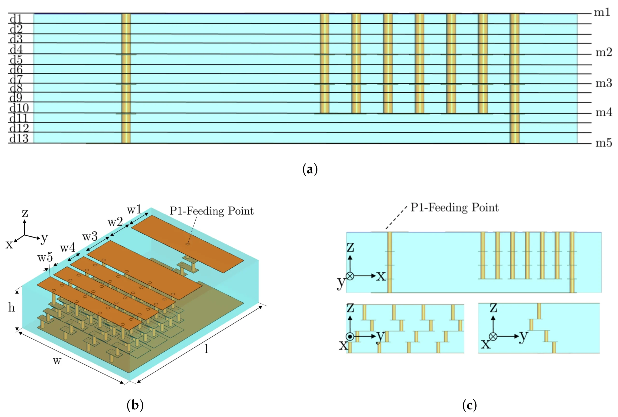
As the opening visual guide of the article, this diagram concretizes the abstract concept of “ground clearance.” It likely depicts the spatial relationship between the antenna element and the continuous ground copper below, possibly with key distances annotated, laying the foundation for subsequent discussions on clearance sizing rules, wavelength fractions, and layout practices.
In every compact 2.4 GHz IoT device, the ground clearance beneath the antenna defines whether the signal travels cleanly or fades halfway across the room. As detailed in TEJTE’s Wi-Fi Antenna Guide, return-current paths and dielectric spacing have as much influence as gain numbers.
Clearance simply means the gap between the radiating structure and the ground plane or metal parts. Too tight, and the field collapses; too wide, and impedance drifts. Most layout issues—especially with FPC antennas—come from ignoring this invisible zone during enclosure design.
This article distills practical sizing rules, keep-out geometries, and routing practices that ensure your prototype’s performance survives final assembly. You’ll also find a decision table for ordering and a Ground-Clear & Keep-Out Quick Estimator to validate your layout before release.
Which Internal Antenna Type Benefits Most from Ground Clearance?
FPC vs PCB vs Ceramic — Who Gains the Most?
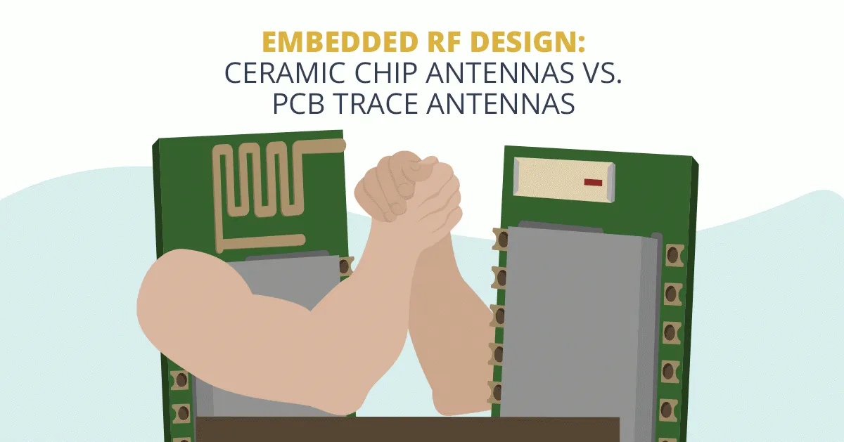
Located in the section comparing different internal antenna types (FPC, PCB, Ceramic), this diagram helps engineers quickly understand that flexible (FPC) antennas are most affected by clearance, while ceramic antennas rely more on precise tuning. The chart format (possibly a radar or bar chart) transforms the qualitative descriptions in the text into a visual representation of trade-offs, aiding early-stage technical selection decisions.
Among internal options, the FPC antenna benefits most from generous clearance. Its thin polyimide substrate easily couples to nearby ground or battery cans; even a 2 mm shift can move resonance by > 80 MHz.
A PCB antenna performs more predictably when its edge ground cut follows design notes—see the comparisons in RF Antenna Types Explained. Ceramic chip antennas, on the other hand, rely on a fixed ground plane; spacing errors mainly affect tuning rather than efficiency.
Rule of thumb:
The freer the antenna (FPC on housing wall), the more clearance-sensitive it becomes.
The more embedded it is (ceramic edge mount), the more tuning-sensitive it is.
Enclosure Plastics and Window Size Sensitivity
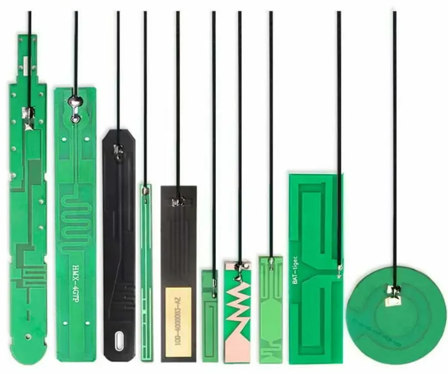
This diagram provides a visual supplement to the specific forms within the “PCB antenna” category. It likely presents the geometric shapes of several common PCB antenna structures, helping readers build an intuitive impression and contrasting with the earlier discussion on FPC and ceramic antennas. It emphasizes that despite their relative stability, the design diversity of PCB antennas and their interaction with plastic enclosures still require careful consideration.
Material choice alters how much clearance you truly have. ABS absorbs more RF energy than PC, and metallic paints can detune antennas beyond recovery. For a 20 × 30 mm antenna window, aim for 6–8 mm air gap behind the FPC foil and avoid any EMI coating nearby.
For PCB antennas buried behind opaque housings, model the plastic’s dielectric constant (~ 3) and expect 1–2 dB efficiency loss compared with open-air tuning. Many engineers use rib-cutouts in the mold to create pseudo-clearance without enlarging the enclosure—an approach proven in multiple TEJTE 2.4 GHz Antenna Selection Guides.
How Do You Size Ground Clearance and RF Keep-Out for 2.4 GHz?
Start from Wavelength Fractions and Refine with Samples
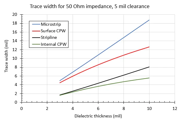
This diagram delves from the macroscopic discussion of ground clearance into the micro-level of transmission line design. Providing quantifiable design guidelines in the form of curves (possibly comparing different structures like microstrip and coplanar waveguide), it serves as a key tool bridging “clearance target values (e.g., λ/20)” with specific PCB stackup design, highlighting the importance of precise impedance control for maintaining RF performance.
Begin with these empirical targets:
- Ground-clear target ≈ λ / 20 ≈ 6 mm (minimum)
- Keep-out target ≈ λ / 12 ≈ 10–15 mm, adjusted per housing
Prototype at those distances, measure S11, then trim layout only after validation. Even shrinking clearance to 4 mm may work if you fine-tune the matching network, but always retest inside the final plastic shell. Extending to 8 mm often yields an extra 0.5–1 dB efficiency gain—small on paper, noticeable in the field.
Metal Proximity Rules and Spacing Tiers

This diagram is a crucial visual aid for understanding metal proximity effects. It clearly separates the antenna radiating layer, the dielectric (PCB), and the rear metal body, possibly using field lines or annotations to emphasize that insufficient distance leads to field compression or resonance frequency shift. It provides the physical context for the subsequent table’s millimeter-level spacing recommendations for different metal components like batteries and shields.
| Metal Part | Recommended Spacing (mm) | Effect if Closer |
|---|---|---|
| Battery pack | ≥ 8 mm | Resonance shift > 100 MHz |
| Shield can | ≥ 6 mm | Pattern distortion, gain loss |
| Display FPC with ground | ≥ 10 mm | Coupled surface currents |
| Screw boss / post | ≥ 3 mm | Local null in pattern |
What Feed Routing Choices Minimize Detuning Near the Ground Plane?
U.FL Tails — Bend Radius and Clamp Points
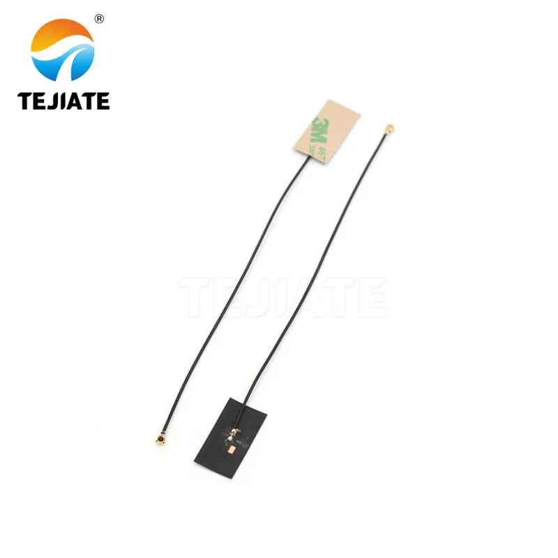
This product image materializes the earlier textual description of “U.FL tails.” It gives readers an intuitive understanding of the physical form (diameter, connector size) of this critical yet fragile connecting component in practical applications, thereby fostering a better grasp of the importance of subsequent engineering rules regarding minimum bend radius (≥5x diameter), air gap, and strain relief.
Tiny U.FL 2.4 GHz tails (0.81 mm or 1.13 mm micro-coax) often break perfect lab tuning once bent sharply or routed across a split ground. Follow these practical rules:
- Maintain bend radius ≥ 5 × cable diameter.
- Keep at least 2 mm air gap from any ground pour.
- Clamp only on the outer jacket, not near the crimp.
- Add a strain-relief loop near the module for vibration endurance.
Each connector interface adds ≈ 0.15 dB loss; each cm of cable ≈ 0.006–0.008 dB. Keep runs under 10 cm when possible. Proper routing details are expanded in the 2.4 GHz Antenna Selection & Ordering Guide.
Short Jumpers to Panel SMA/RP-SMA vs Direct U.FL
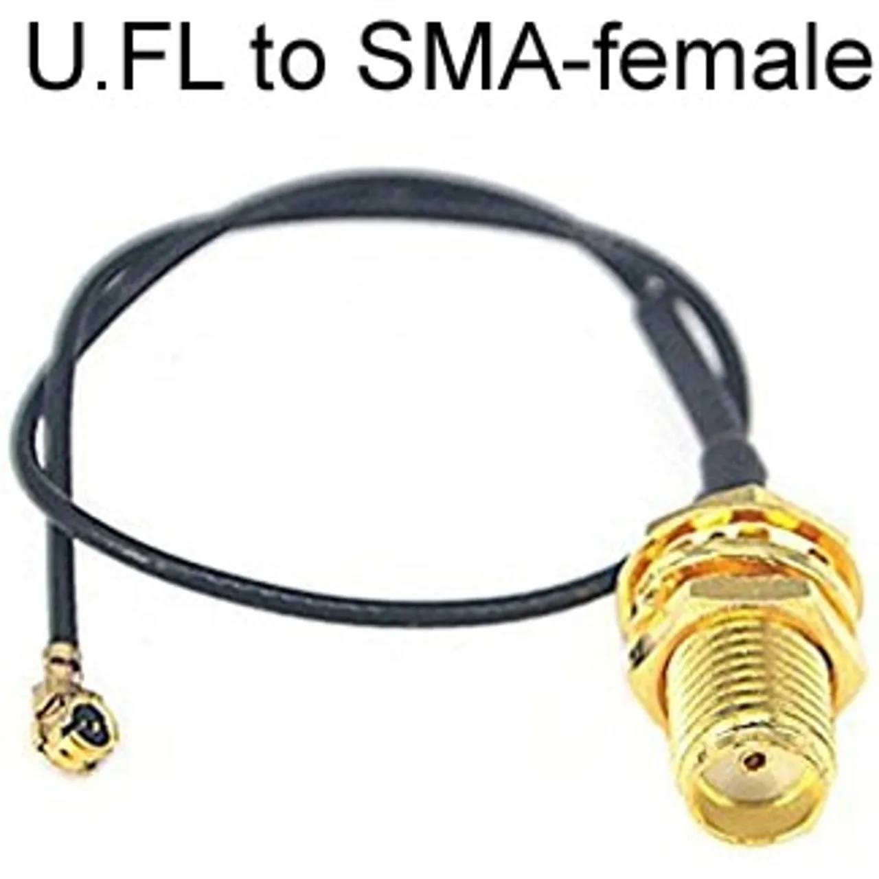
This image serves as a physical reference for making the “convenience vs. performance” trade-off decision. It clearly shows a complete U.FL-to-SMA conversion chain, making the concept of “extra connector pairs” concrete. Engineers can use this to visually assess whether introducing such an adapter for debugging convenience is acceptable given its performance cost in specific applications (e.g., low-power devices).
Adding a panel SMA or RP-SMA offers convenience but introduces two extra interfaces and roughly 0.3 dB total loss. For low-power radios such as nRF52 or ESP32, that may cut your range by 10–15 %. Direct U.FL connections minimize loss but demand disciplined strain relief and careful internal clearance.
When specifying feeds for manufacturing:
• Cable type: 0.81 / 1.13 mm micro-coax
• Length: ≤ 150 mm total
• Connector pairs: ≤ 2
All these parameters will feed directly into the estimator table in the ordering section. For deeper mechanical routing tips, see TEJTE’s RF Antenna Types Explained.
Will Cable Type and Length Quietly Erase Your Link Margin?
0.81 mm vs 1.13 mm Micro-Coax — The Hidden Tradeoff
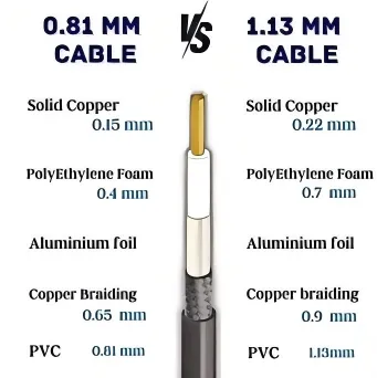
| Cable Type | Typical Loss (dB/cm @ 2.4 GHz) | Max Bend Radius | Typical Application |
|---|---|---|---|
| 0.81 mm | 0.008 dB/cm | ≥ 4 mm | Ultra-compact wearables, BLE beacons |
| 1.13 mm | 0.006 dB/cm | ≥ 6 mm | Wi-Fi modules, mid-sized IoT devices |
A 10 cm 0.81 mm cable with two U.FL pairs already costs you around 0.26 dB total loss. Double the length, and you lose over half a decibel—enough to push a borderline BLE link into retransmission territory.
That’s why TEJTE’s 2.4 GHz Antenna Selection & Ordering Guide always pairs FPC antennas with short 1.13 mm tails when the housing allows. The gain-to-loss balance is often better than shrinking the cable diameter just to save routing space.
“Gain vs Feeder Loss” Sanity Checks Before Freezing the BOM
Before you lock the bill of materials, do a quick link-budget sanity check:
- Start with your nominal antenna gain (e.g., +2 dBi).
- Subtract cable + connector losses (e.g., –0.4 dB).
- Compare to the module’s conducted power – regulatory limits (~18 dBm).
- Estimate free-space range using 20 log d + 20 log f + 32.44 = link budget margin.
If the resulting margin falls below 10 dB for your worst-case environment, shorten the cable or change to the 1.13 mm type. TEJTE engineers frequently find that shortening one cable saves more performance than retuning the antenna itself.
For outdoor or waterproof products with SMA panels, consult the Omnidirectional Antenna Selection Guide—its examples show how to keep total loss under 1 dB even through bulkheads.
Can You Tune Matching (Pi/L) Without Over-Fitting to One Prototype?
S11 Targets and Coarse-to-Fine Iteration
This diagram concretizes the operation of “matching network tuning.” It likely displays a circuit layout containing multiple parallel or series capacitors/inductors, emphasizing the use of discrete, replaceable components for “coarse tuning” rather than relying on a single precision variable capacitor. This embodies a robust engineering philosophy: approaching the target through structured steps to ensure results are repeatable across multiple samples.
Every matching network aims for a return loss better than –10 dB (S11) across 2.4–2.5 GHz. But chasing perfection on one golden unit is risky. Adhesive thickness, plastic curvature, or flex cable strain can shift resonance by 50 MHz or more.
The better approach is iterative:
- Coarse tune using a wide trace cut or tunable capacitor bank.
- Mount inside the enclosure and measure again—don’t trust open-air results.
- De-embed the feed cable loss before judging S11.
- Once inside –10 dB across the band, stop fine-tuning unless multiple samples confirm repeatability.
Over-tuning to one board often leads to mass-production failures. In FPC Antenna Guide: 2.4 GHz Layout & Tuning, TEJTE highlights a real case where matching caps optimized for one prototype worsened performance across ten others by 2 dB.
Production Variability: Adhesives, Plastics, and Temperature Drift
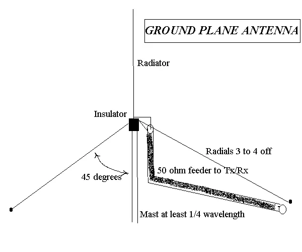
This diagram introduces a fundamental model in antenna engineering. It shows the principle of artificially creating “clearance” through a physical structure (insulating mast), echoing the concept of “ground cut” in PCB design. It helps readers understand that ground clearance is not merely a two-dimensional planar distance issue but can also be achieved through three-dimensional structures, offering ideas for solving antenna layout problems in compact spaces.
Small variations in adhesive foam density, plastic dielectric, or ambient temperature change antenna resonance slightly. Expect:
- ± 30 MHz shift per °C in extreme cases.
- ± 1–1.5 dB swing when switching between matte and glossy plastics.
- Up to 3 dB difference between dry lab and humid outdoor tests.
To stabilize results:
- Use consistent adhesive types (Acrylic vs silicone).
- Record installation torque and alignment on drawings.
- Validate at 0 °C / 25 °C / 60 °C for production qualification.
A controlled adhesive area and ground-clear spec should both appear in your PO—a practice detailed later in the Order Like a Pro matrix.
Where Should You Place the Antenna Window Relative to Ground and Metal?
Ground Cut vs Ground Clear — Patterns and Return-Path Hygiene
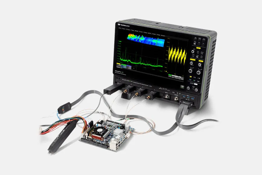
This physical testing photo emphasizes that “design must consider real-world usage scenarios.” It connects the abstract concept of “human body detuning” with a specific test setup, reminding engineers that the impact of hand grip must be considered during layout and verification stages, and can be mitigated by placing the antenna at the device edge or adding an air gap.
When you can’t raise the antenna high above ground, the next best solution is to cut the ground under it. But not all cuts are equal.
- A continuous rectangular void provides predictable isolation but may complicate routing.
- A slot-type cut (thin gap between antenna trace and ground pour) balances mechanical strength and RF separation.
- For FPCs attached to housing plastic, the “ground clear” area under the antenna must extend at least 6 mm beyond its footprint.
Avoid floating copper islands—they create parasitic resonances. Instead, tie the surrounding ground to chassis via multiple vias every 5 mm. TEJTE’s RF Antenna Types Explained shows cross-sections of correct return-path stitching that keep the current symmetric.
Human-Body Detune and Hand-Grip Experiments for Handheld IoT

This diagram visualizes the estimation tool described in the text. It integrates the scattered design rules (λ/20 clearance target, cable loss coefficients, connector loss) into a logical tool interface, demonstrating how to assess layout risk through systematic inputs. It serves as a key bridge connecting theoretical rules with engineering practice, embodying a data-driven decision-making approach.
The human body detunes 2.4 GHz antennas heavily. Conductive tissue acts like a lossy dielectric with ε ≈ 45. When designing handheld products:
- Assume 1–2 dB efficiency loss when gripped.
- Test with the enclosure held in both left and right hands.
- Keep at least 15 mm between antenna and main board battery cell.
For wearable or portable sensors, offset the antenna window to the upper edge or corner so that the user’s hand or wrist covers less of the field. Even small repositioning can recover 3 dB of effective gain.
During field trials, record RSSI variance across users—real data often exposes coupling issues missed in simulation. As noted in TEJTE’s Wi-Fi Antenna Guide, the best fix isn’t higher gain, but cleaner field symmetry through better ground control.
Do You Need to Switch from FPC to PCB/Ceramic for This Product?
When Mechanical Constraints Limit Clearance
Coexistence with Wi-Fi, BT, and Thread
When multiple radios share 2.4 GHz, keep their antennas separated by at least 15 mm edge-to-edge or one-quarter wavelength for best isolation. Multi-band modules sometimes embed all three networks on one port, but spacing still matters for desense prevention.
If your layout can’t provide that separation, consider time-domain multiplexing or filtered RF switch matrices—both available in TEJTE’s component portfolio for OEMs needing certified coexistence.
Order Like a Pro: What Must Be on Your PO and Drawings?
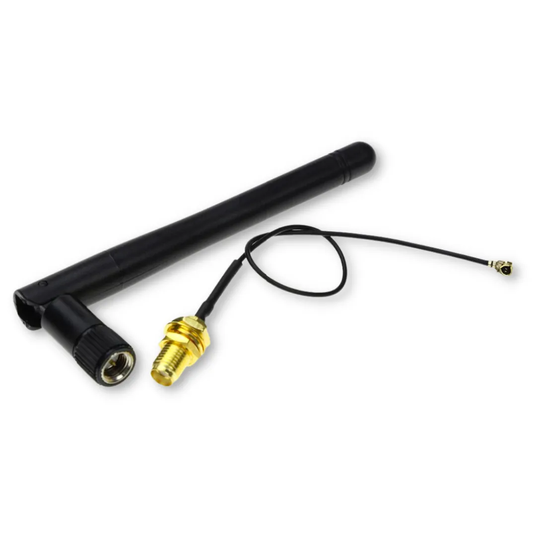
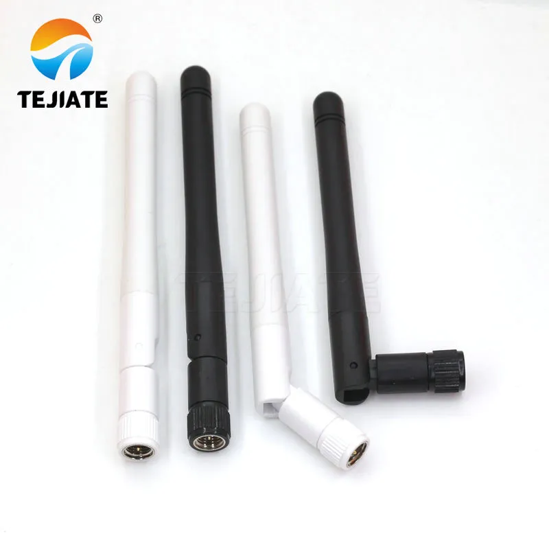
This product image connects all the preceding technical discussions (clearance, loss, matching) with a procurable specific SKU. It shows the typical external form of such an antenna (flexible rod, connector, cable), making the various fields in the ordering matrix (e.g., “Antenna Type,” “Cable Type/Length”) concrete and tangible, reducing ambiguity in the procurement process.
Every well-built RF antenna purchase order shares one trait: it reads like an engineering spec, not a casual email. Missing details about ground clearance, adhesive, or cable type are what usually derail first-build samples.
Below is a compact Ground-Clear & Keep-Out Quick Estimator, followed by an Ordering Matrix template you can drop directly into your BOM or drawing notes.
A. Ground-Clear & Keep-Out Quick Estimator
| Parameter | Typical Range | Description |
|---|---|---|
| freq_GHz | default = 2.4 | Operating frequency |
| antenna_type | FPC / PCB / Ceramic | Layout choice |
| window_size_mm | 20 – 60 | Plastic opening or FPC area |
| adjacent_metal_mm | 0 – 15 | Nearest metal distance |
| cable_type | 0.81 / 1.13 mm | Micro-coax diameter |
| cable_length_cm | 5 – 20 | Tail length |
| connector_pairs | 1 – 3 | Number of U.FL / SMA pairs |
Constants (@ 2.4 GHz)
λ = 125 mm
loss_per_cm (0.81) ≈ 0.008 dB
loss_per_cm (1.13) ≈ 0.006 dB
connector_loss ≈ 0.15 dB per pair
Heuristic Targets
ground_clear_target = max(λ / 20, 6 mm)
keep_out_target = max(λ / 12, 10 mm)
Loss Calculation
cable_loss = loss_per_cm(type) × cable_length_cm
conn_loss = connector_pairs × 0.15 dB
Risk Score (0–10)
risk = f(ground_clear_target − actual_clear,
keep_out_target − actual_keepout,
adjacent_metal_mm,
cable_loss + conn_loss)
If risk ≥ 6 → Redesign or shorten tail / enlarge window before mass build.
B. Ground-Aware Ordering Matrix
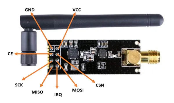
This module diagram represents the “black-boxing” trend in modern RF design. It shows a module integrating the chip, matching circuit, and a standard antenna interface, emphasizing its pre-certified and fixed-layout characteristics. The diagram reminds engineers that while using such modules simplifies certification, the clearance and layout requirements in their reference design must be strictly adhered to and cannot be arbitrarily altered.
| Field | Example Entry | Purpose |
|---|---|---|
| Antenna Type | FPC 2.4 GHz | Identify design family |
| Ground-Clear (mm) | ≥6 | Clearance zone under element |
| Keep-Out (mm) | ≥ 12 | No copper or metal in zone |
| Adhesive Area / Spec | 3M 9448A tape | Defines attachment & dielectric |
| Cable Type / Length (cm) | 1.13 mm / 10 cm | Loss control |
| Connector Type | U.FL / SMA JK | Interface |
| Exit Angle | 90° / 180° | Cable routing |
| Temp Range | -40 ~ 85 °C | Environment |
| Compliance | RoHS / REACH | Regulation |
| Labeling | TEJTE PN & date code | Traceability |
| TEJTE SKU | ANT-FPC-24-113-10 | Internal match |
| Lead Time | 2 - 3 weeks | Planning |
| MOQ | 50 pcs | Procurement |
| Notes | Torque 0.3 N-m / PE bag pack | Assembly |
What’s New in 2024 – 2025 That Affects Internal Antenna Clearance?
Tri-Band Clients vs Low-Power IoT
Wi-Fi 7 and Thread gateways now crowd 2.4 GHz with tri-band clients. That means your tiny IoT module might coexist beside high-EIRP routers inside the same chassis. The best defense is still clean ground isolation—≥ 6 mm cut and ≥ 15 mm separation between radio modules.
Modern pre-certified modules often embed a standardized U.FL tail and matching keep-out ring in their reference Gerbers. Reusing those footprints, as shown in TEJTE’s FPC Antenna Guide: 2.4 GHz Layout & Tuning, saves months of trial-and-error.
Standardized Tails and Reduced Layout Variance
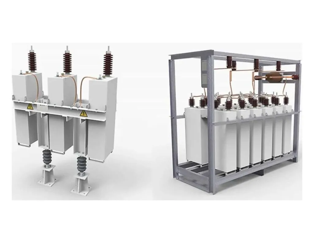
As the concluding visual element of the article, this diagram employs a cross-domain analogy (power transmission lines) to present complex RF layout principles in a more accessible and vivid manner. It reinforces the idea that “clearance is a safety boundary,” and likely deepens the engineering principle of caution by annotating elements like “Lowest Conductor,” “Sag,” and “Ground Clearance,” providing a vivid endpoint to the entire text.
Module vendors are moving toward pre-tuned antenna kits with fixed cable lengths and adhesive spec—effectively “locking in” the RF path. It minimizes layout variance but also means your mechanical team must follow the exact clearance recipe. Deviate by even 2 mm and certification data becomes invalid.
By aligning your design to these standardized kits, you can push projects through FCC / CE faster. TEJTE’s component library now reflects those updated dimensions to simplify integration across BLE, Zigbee, and Wi-Fi 6/7 platforms.
FAQ — Ground Clearance & Internal Antennas
How much ground clearance is “enough” around a 2.4 GHz internal antenna?
Does a ground cut (slot) work better than a full void near the window?
How close can a battery or metal shield sit next to the antenna edge?
How long can a 0.81 mm or 1.13 mm U.FL tail be before link margin collapses?
Should I route to a panel SMA / RP-SMA or keep U.FL inside the enclosure?
What S11 target should I use and how do I avoid over-tuning?
How can I validate clearance quickly during layout?
Takeaway
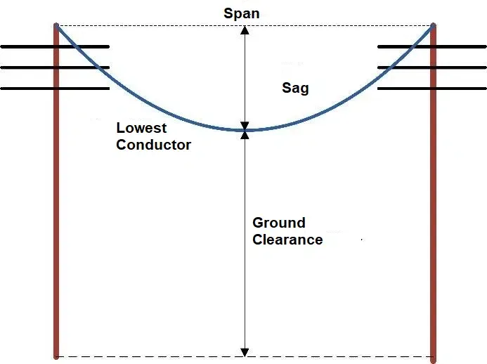
This diagram transcends specific technical parameters, employing a cross-domain analogy (power transmission) for conceptual elevation. It visualizes the abstract principle of “design safety margin,” vividly conveying that, regardless of the specific calculation, reserving interference-free physical space (i.e., clearance) for RF energy is as fundamental to ensuring reliable and stable system operation as maintaining safety distance from the ground is for high-voltage power lines. It provides the entire technical guide with a core visual metaphor that is easy to remember and disseminate.
Ground clearance is one of those invisible parameters that decides whether your 2.4 GHz product passes certification on the first try—or spends months in debug.
Follow the λ / 20 rule, preserve a clean return path, and record every spec in your drawings. When in doubt, rerun the estimator and cut another millimeter of ground. It’s cheaper than chasing ghosts later.
For more implementation examples, see:
Bonfon Office Building, Longgang District, Shenzhen City, Guangdong Province, China

A China-based OEM/ODM RF communications supplier
Table of Contents
Owning your OEM/ODM/Private Label for Electronic Devices andComponents is now easier than ever.
