Flyback Diode Guide for 12 V Systems
Nov 30,2025
How do you size a flyback diode for a 12 V rail?
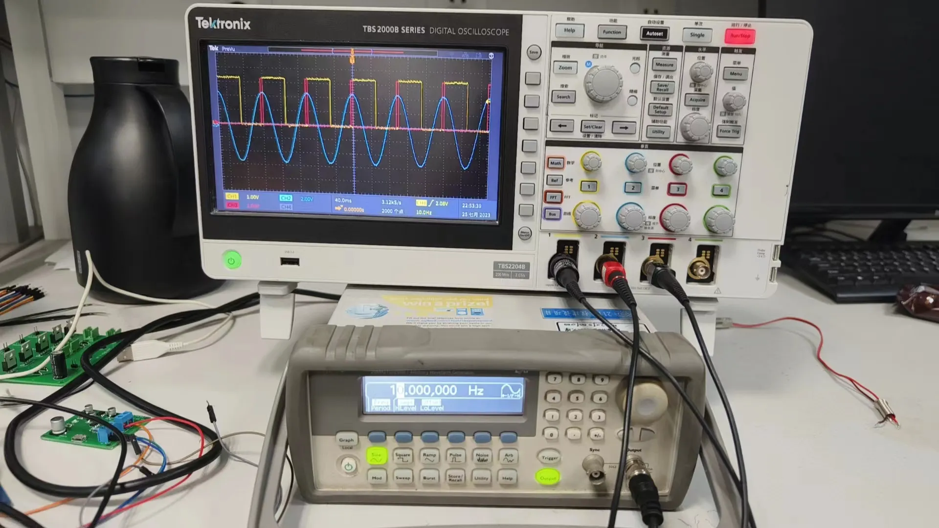
Figure establishes the conceptual foundation for the entire document, using a concise diagram to help readers quickly understand the scenario and importance of the flyback diode, emphasizing its small yet critical protective role.
When designing a 12 V system, one small device quietly guards the entire rail — the flyback diode. It’s easy to overlook, yet it determines whether your MOSFET, relay driver, or power switch survives the next inductive kick.
Sizing it right isn’t guesswork; it follows a logical process grounded in current, voltage, and heat.
Step 1 — Find the coil or motor current first(DC relay vs PWM motor)
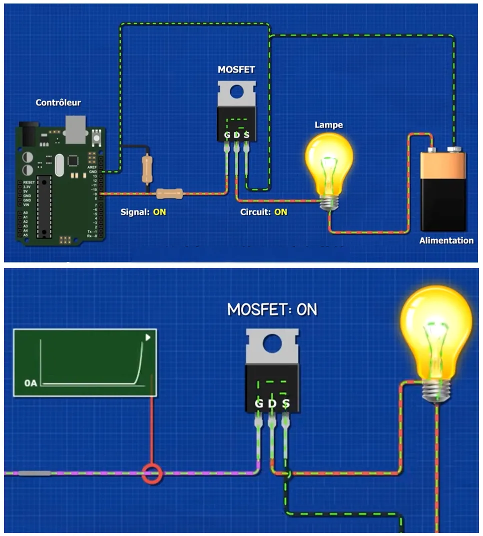
Figure serves as the starting point for theoretical analysis, concretizing the abstract concept of "inductive load" into an analyzable circuit model, providing clear circuit context for subsequent calculations of the diode's required current (average current, surge current).
Before reading any datasheet, quantify the load.
- For a DC relay coil, use its rated coil current — typically 50 to 200 mA for signal relays, up to 1 A for automotive types.
- For a PWM motor or solenoid, estimate an RMS or duty-weighted current ( I_load × Duty %) since the diode conducts during every off-cycle.
That gives the minimum IF(AVG) the diode must handle. Always include margin because inductive loads spike when released.
For instance, a 12 V relay drawing 80 mA needs a diode that can handle at least 0.1 A average. The surge current (IFSM) should be several times higher to cover release peaks.
When that current loops through your MOSFET driver, the stress path mirrors what’s seen in a Logic-Level MOSFET for 12 V Loads setup — same physics, different part.
Step 2 — Pick VR, IF(AVG), IFSM and T J with margin
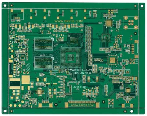
Figure transforms the selection rules from a text table into a visual chart, allowing engineers to more intuitively understand the interrelationships between parameters and design margins. It is a key tool bridging theoretical calculations and physical component selection.
| Parameter | Rule of Thumb | Purpose |
|---|---|---|
| VR (Reverse Voltage) | ≥ 2 × Vbus to ≥ 24 V for a 12 V rail | Survive inductive overshoot |
| IF(AVG) | ≥ Iload × Duty | Average current support |
| IFSM | ≥ 2 × surge/lock-rotor current | Handle kickback spikes |
| TJ / Thermal Budget | P = Vf × Iavg → ΔT = P × RθJA | Prevent thermal runaway |
A 60 V / 1 A Schottky such as PMEG6010CEJ,115 has Vf ≈ 0.66 V @ 1 A and leakage ≈ 50 µA @ 60 V.
Power loss ≈ 0.66 W; on a small SOD-323F pad (θ JA ≈ 150 °C/W) the junction can rise by ~100 °C unless the PCB has ≥ 1 cm² copper pour.
That’s why TEJTE’s RF Coaxial Cable Guide also emphasizes thermal path continuity — the principle is identical for power devices.
Step 3 — Schottky or fast-recovery? Know the trade-off
| Type | Vf Range | Reverse Recovery (Qrr) | EMI Behavior | Best Use |
|---|---|---|---|---|
| Schottky | 0.3 – 0.7 V | Near zero | Very quiet | ≤ 60 V rails, 12 V flyback loops |
| Fast Recovery | 0.7 – 1.2 V | Moderate | Some ringing | > 60 V systems or hot environments |
A Schottky flyback diode minimizes heat and noise, making it ideal for compact 12 V controllers.
Yet in a hot automotive bay, where leakage rises exponentially above 125 °C, a fast-recovery rectifier can be the safer option.
You’ll see the same balance when designing the NCP1207 Flyback Converter — efficiency and switch recovery always interact.
Freewheel diode vs TVS — which protects relays and motors better?
Typical use cases
- Relay coil to flyback diode across coil suppresses ~200 V spikes.
- DC motor to diode plus RC snubber tames broader EMI spectrum.
- Solenoid to requires higher IFSM rating for stored energy.
- Buck/Flyback converter to low Vf and fast Qrr matter more than energy storage.
In automotive 12 V rails, a combination of freewheel diode + TVS offers the best protection and is discussed in the TVS Diode for Automotive 12 V post.
Placement matters — minimize loop area and lead inductance
Even a perfect diode fails if it’s placed wrong. Put it directly across the inductive load’s pins and keep the loop tight. Long traces add inductance that amplifies ringing and can cause false scope readings.
Use wide tracks or short vias to maintain a low-impedance path — it’s the same discipline you’d apply to SMA to BNC Lab Wiring where signal integrity depends on loop geometry.
What if the diode slows release time?
A basic diode keeps current flowing until the field collapses, so relays or solenoids open slower.
If response speed matters:
- add a Zener in series (reverse-oriented) to raise clamp voltage,
- use an RC snubber to absorb energy, or
- adopt a transorb TVS for faster decay.
Each method trades off slightly higher switch stress for faster release — just verify V DS margins.
Can small packages (SOD-323F / 1 A) handle real 12 V loads?
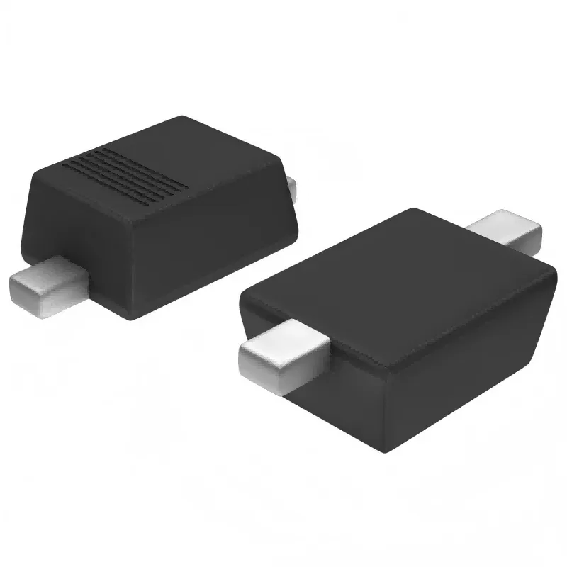
Figure provides valuable real-world application reference, translating the package dimensions from the device datasheet into a real visual scale. It helps engineers evaluate the feasibility of its application in compact spaces and intuitively understand the critical impact of good thermal layout (e.g., sufficient copper area) on the reliability of small-package devices.
| Parameter | Typical Value | Practical Meaning |
|---|---|---|
| VR | 60 V | Provides ≥ 2× 12 V margin |
| IO | 1 A | Suitable for small relays or PWM fans |
| VF | 0.66 V @ 1 A | Low loss, cooler operation |
| trr | ≤ 500 ns | Fast enough for switching loads |
| IR | 50 μA @ 60 V | Negligible leakage |
| Cj | 68 pF @ 1 V, 1 MHz | Predictable AC behavior |
| TJ,max | 150 °C | High thermal headroom |
| MSL Level | 1 | Unlimited shelf life for reflow |
| RoHS / REACH | Compliant / Not affected | Export-safe |
| ECCN / HTSUS | EAR99 / 8541.10.0080 | No export restriction |
Design Rules, PCB Placement & Lifecycle Updates
Do selection rules change between buck, flyback, and reverse polarity protection?
Buck / flyback output rectifier stress
In a buck converter, the diode conducts every switching cycle, carrying the inductor current during the MOSFET’s off-time. That means its IF(AVG) and IF(RMS) values are continuous, not just transient.
The current ripple, switching frequency, and junction temperature all determine lifetime. A Schottky rectifier minimizes switching loss because of its negligible recovery charge (Qrr). But you must also ensure its reverse voltage (VR) covers double the output plus spikes.
In a flyback topology, reverse recovery dominates EMI behavior. Designers often pair the diode with an RC snubber or use a fast-recovery diode when the secondary voltage exceeds 60 V.
If you’re already using NCP1207-based flybacks, the same logic appears in TEJTE’s Flyback Converter Design Guide—where diode Qrr directly affects efficiency and transformer stress.
Reverse polarity protection on 12 V rails
When the diode sits in series with the supply, its role flips. Instead of absorbing spikes, it blocks reverse connection.
Here, forward drop (Vf) and thermal resistance dominate:
- A Schottky diode keeps Vf low (~0.3–0.7 V), but watch power loss: P = Vf × I.
- In high-current systems (3–5 A automotive rails), conduction loss becomes unacceptable.
- That’s why many engineers now switch to MOSFET OR-ing or ideal-diode controllers—giving the same polarity protection with minimal voltage loss.
For medium-current loads (≤ 1 A) a reverse polarity protection diode like PMEG6010CEJ,115 still works well, especially when board space is limited and transient tolerance (60 V rating) is sufficient.
EMI & ringing control around the diode loop
Each fast edge can excite stray inductance. The smaller the loop between switch and diode, the less ringing appears on your scope.
If you ever see oscillations above 50 MHz on the switch node, try:
- Shortening the return path;
- Adding a snubber (R + C in series across the diode);
- Or replacing the device with a “soft-recovery” rectifier — a middle ground between Schottky and ultrafast types.
These practices mirror good RF layout discipline; see how trace geometry affects reflections in TEJTE’s SMA to BNC Adapter Guide — it’s the same story, just at DC or kHz scales.
Where should you place and test the diode on a compact PCB?
Loop placement checklist for relays / motors / DC-DC
- Keep diode as close as possible to inductive terminals.
- Use wide copper pour for both current and heat spreading.
- Avoid long detours through vias—each adds nH of parasitic inductance.
- For multi-channel boards, dedicate isolated return loops per load.
A well-placed freewheel diode not only protects your switch but also reduces radiated noise that might otherwise couple into signal lines.
Oscilloscope probing — ground spring and coax tip
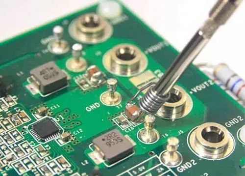
Figure emphasizes a critical practical technique in high-frequency switching circuit measurement. Incorrect probing methods (e.g., using long ground leads) introduce additional inductance, leading to observed false ringing and overshoot that can mislead debugging. By showing the correct equipment connection method, this figure teaches engineers how to avoid “chasing ‘ghost’ EMI” and ensures measurement accuracy. It is an important reference for effective circuit validation and fault diagnosis.
When verifying the flyback event, probe right at the switch node with a short ground spring.
Avoid long ground leads; they introduce inductance and fake “ringing.”
A 200 MHz scope with coax probe tip shows a true waveform of voltage overshoot and diode recovery.
Engineers often forget this step and chase “ghost” EMI that only existed in the probe loop.
For test-bench cable setup, reference TEJTE’s RF Coaxial Cable Guide; the same grounding logic applies to low-frequency switching nodes.
Pass / fail criteria — overshoot, ringing, temperature rise
After a few minutes under full load:
- Overshoot < 2 × Vbus (24 V typical limit for 12 V rails)
- Ringing damped within one cycle
- Temperature rise < 80 °C above ambient
If any exceed those limits, upgrade the diode package (SOD-323F to SOD-123 or SMB) or improve copper thermal area.
Use small thermocouples on the diode case for accurate readings—IR cameras often over-estimate reflections.
What’s new for PMEG6010CEJ,115 users? (PCNs & sourcing updates)
| Date | Change / Notice | Impact / Action |
|---|---|---|
| 02-Nov-2015 | Bond wire Au to Cu conversion | No electrical impact, but update process docs |
| 01-Jan-2019 | Wafer fab source change | Cross-check lot mark for consistency |
| 02-Aug-2020 | Label format update for all devices | Revise incoming inspection criteria |
| 12-Jun-2024 | Mult-device label change | Verify barcode recognition in reel feeders |
| 24-Apr-2025 | CNR manual reel hub diameter update | Affects auto-taping settings only |
| 06-Aug-2025 | Design update for mark clarity | Visual marking difference only |
| 06-Nov-2025 | Additional assembly site release | Add new site to LCR approval list |
All revisions keep the device electrically identical (Vf ≈ 0.66 V @ 1 A, IR ≈ 50 µA @ 60 V, Cj ≈ 68 pF), maintaining full RoHS3 and MSL1 status.
If your process includes automotive-grade sourcing, consider the upcoming QX variant for AEC-Q101 compliance.
Before any mass build, verify the lot mark and assembly site against the latest PCN. TEJTE’s component engineers often recommend logging those in your ERP BOM alongside the Flyback Diode Selection Guide for traceability.
Quick Selector & Design Wrap-Up
Build a quick, defensible pick in 2 minutes
Selecting the right flyback diode shouldn’t take an hour of spreadsheet work.
Below is a practical “12 V Diode Quick Selector” workflow that lets you estimate thermal margin and package suitability in under two minutes.
| Input Field | Example Value | Comment / Formula |
|---|---|---|
| Rail Voltage Vbus | 12 V | Supply voltage of system |
| Load Type | Relay | Relay / Motor / Solenoid / Buck / Flyback |
| Iload (A) | 0.25 A RMS | Steady or RMS current |
| Duty (%) | 50 % | PWM or effective duty cycle |
| Ambient Ta (°C) | 40 °C | Expected operating temperature |
| Board Copper | 1/2 oz, 1 cm² | Defines θ JA,eff |
Calculation logic
VR_min = 2 × Vbus to choose ≥ 24 V for a 12 V rail
IF(AVG) ≈ I_load × Duty
P_diode ≈ Vf(@IF) × IF(AVG)
ΔT ≈ P_diode × θJA_eff
IFSM_check ≥ 2 × inrush / pull-in current
PASS ⇨ if (ΔT + T_a) < (TJmax – 20°C) and VR, IF, IFSM within rating
else to step up package (SOD-323F to SOD-123 to SMB)
Example Output
| Package Tier | Verdict | Recommended VR | Example Part Number |
|---|---|---|---|
| SOD-323F / SOD-123 | PASS (thermal OK @ 0.25 A) | ≥ 60 V | PMEG6010CEJ,115 |
Engineers using compact relays or PWM fans can plug their own numbers into this table and instantly see whether a Schottky rectifier still fits or needs a thermal upgrade.
A similar decision tree is also featured inside TEJTE’s Power-and-Protection Hub for consistent component evaluation.
Practical validation with PMEG6010CEJ,115
On a small controller board, a single PMEG6010CEJ,115 can serve both as a freewheel diode for a relay and as a reverse-polarity protection diode on the input line.
That flexibility comes from its 60 V VR, 1 A Io, and fast ≤ 500 ns recovery.
Lab Tips
- Thermal Test — Drive a 12 V relay (80 mA) with 10 Hz PWM. Measure diode temperature with a micro thermocouple.
- Scope Waveform — Observe the switch node using a coax tip and ground spring; you should see a smooth decay without overshoot beyond 2× Vbus.
- Layout Check — Keep trace length < 10 mm from coil to diode; any longer adds inductive ringing.
- Alternate Package Rule — If ΔT > 100 °C on your board, move to SOD-123 or SMB package with same electrical rating.
Because the device is RoHS3 compliant, MSL 1 rated, and classified EAR99, it fits international production without export restrictions. Its reliability and low Vf make it a popular choice across 12 V automation, IoT, and lab equipment segments.
For more complex power chains (such as combining TVS and flyback paths), you can reference TEJTE’s dedicated TVS Diode for Automotive 12 V article for layered protection strategies.
Frequently Asked Questions (FAQ)
1. How much reverse-voltage margin should I allow for a 12 V flyback diode?
Always give yourself at least 2× the bus voltage.
For a 12 V rail, choose a diode rated ≥ 24 V, but 60 V is a safer standard since real-world harnesses and coils often generate spikes far beyond nominal. The PMEG6010CEJ,115 (60 V rating) comfortably covers those events without adding unnecessary cost or size.
2. Will a flyback diode slow down my relay or solenoid release?
Yes — a simple diode keeps current circulating until the coil’s field collapses, which delays release by a few milliseconds.
If fast drop-out is critical, replace it with a Zener-assisted clamp or add an RC snubber.
Just make sure your switch (MOSFET or transistor) can withstand the resulting higher voltage across it.
3. Is a 1 A SOD-323F Schottky like PMEG6010CEJ,115 enough for real 12 V loads?
Often yes.
For small relays, solenoids, and PWM fans drawing under 0.3–0.5 A average, it performs well — assuming your PCB provides adequate copper for heat spreading.
In heavier-duty or high-ambient environments, step up to SOD-123 or SMB packages to lower junction temperature.
4. Where exactly should I place a freewheel diode on the PCB?
Right across the inductive load terminals — the shorter the loop, the smaller the overshoot.
Keep traces wide and direct.
If your layout forces distance, consider a small local capacitor or TVS diode near the load to suppress residual ringing.
5. Can a TVS replace my flyback or freewheel diode?
Not really.
A TVS diode reacts only when voltage spikes above its breakdown, clamping the event.
A freewheel diode conducts the actual current and dissipates the magnetic energy.
They complement each other — use both for harsh automotive or relay-heavy systems.
Bonfon Office Building, Longgang District, Shenzhen City, Guangdong Province, China

A China-based OEM/ODM RF communications supplier
Table of Contents
Owning your OEM/ODM/Private Label for Electronic Devices andComponents is now easier than ever.
