ESD Protection Diode: High-Speed Interface Practice & Layout
Dec 13,2025
Introduction — Why ESD Design Still Fails at High-Speed Ports
Serving as the article's cover image in the introduction, this picture uses a real engineering test scene to visually introduce the theme: even today, incorrect ESD protection design for high-speed interfaces can still lead to failure. It emphasizes the importance of combining theoretical knowledge with practical measurement (oscilloscope).
Even after decades of ESD design guides and layout notes, it’s still surprisingly easy to damage a high-speed interface with the wrong ESD protection diode.What used to work for slow GPIO lines often collapses when the data rate hits several gigabits per second. A misplaced via or an oversized TVS diode array can distort the signal eye or fail IEC 61000-4-2 testing before you even finish your prototype.In real-world projects, I’ve seen engineers install a unidirectional TVS on an HDMI port simply because “the breakdown voltage looked right.”On paper, it made sense — but on the oscilloscope, half the signal swing disappeared.
That’s the painful truth: once you’re running at 6 Gbps or higher, ESD protection is no longer just about surviving a surge. It’s about protecting the signal path without destroying its integrity.When working with interfaces such as HDMI 2.1, USB 3.2, or DisplayPort, every diode, trace, and via matters.
This article explains how to choose between unidirectional and bidirectional ESD diodes, how to calculate the capacitance budget, align the clamp voltage to your IC’s maximum ratings, and determine the best placement strategy for consistent protection.
How Do You Choose Between Unidirectional and Bidirectional ESD Diodes?
Choosing the right ESD protection diode always begins with one key question:
Does your interface carry DC bias or not?
If yes, go for a unidirectional diode. If not, you’ll need a bidirectional one.
That rule of thumb works well — but there’s more depth to it.
Three-Step Decision by Interface Type (DC / Single-Ended / Differential)
Here’s a simple three-step process that most engineers use during design reviews:
1.DC lines (power rails, analog sensors)
Always use unidirectional TVS diodes. They clamp in one direction only and avoid reverse leakage when biased.
2.Single-ended data lines (UART, SPI, I2C)
Still unidirectional, but verify your idle voltage.
For example, if your signal idles at 3.3 V, make sure the diode’s working voltage (VWM) is at least 3.6 V to prevent false conduction.
3.Differential pairs (USB, HDMI, LVDS, DisplayPort)
Use bidirectional TVS arrays.
They allow both positive and negative swings while clamping large surges symmetrically.
Think of it this way:
If your signal line always stays above ground, choose a unidirectional device.
If it swings around ground, bidirectional is safer and cleaner.
Polarity Does Not Equal Channel Count
A frequent mistake is assuming a “dual-channel” TVS means it’s bidirectional. That’s wrong.Channel count refers to the number of signal lines in a package, not the voltage polarity each channel supports.I’ve debugged HDMI boards where designers installed two single-direction parts instead of one four-line bidirectional array.The result? Uneven clamp levels and visible signal skew on the eye diagram.
When checking datasheets, look for this clue: if you see two opposing diode symbols meeting at the center node, that’s a bidirectional array.And don’t trust part names blindly — something like ESD5V0D3 might sound bidirectional but isn’t unless the datasheet explicitly says so.
Why Should High-Speed Lines Prefer Low-Capacitance TVS Arrays?
Once your signal speeds pass a few hundred megahertz, capacitance becomes the silent killer.
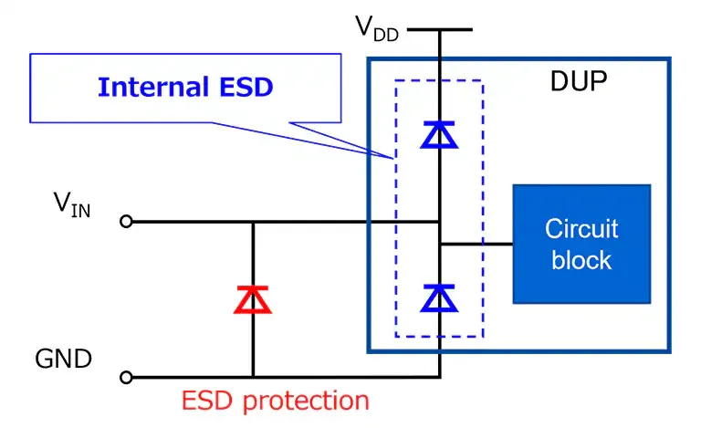
The parasitic capacitance of an ESD protection diode directly loads your transmission line, which slows down the edges, reduces eye height, and increases return loss.
In short: too much capacitance equals a closed eye diagram.
Array vs. Discrete Devices: Routing and Return Path
For modern interfaces like HDMI, USB Type-C, or MIPI, a TVS array integrates multiple protection channels with a shared ground return. Compared with using individual discrete diodes, arrays have several clear advantages:
- Better matching – Each channel has nearly identical parasitics, keeping skew within the differential pair extremely low.
- Smaller loop area – All ESD currents share one common ground, minimizing inductance.
- Simpler routing – One compact package means cleaner differential routing and fewer vias.
Using multiple discrete diodes may look flexible, but it often causes routing chaos and inconsistent capacitance per line.
For most multi-gigabit designs, TVS arrays simply make sense.
Placement and Parasitics
Appearing in the chapter explaining “Why high-speed lines should prefer low-capacitance TVS arrays,” this diagram visually demonstrates the core advantages of arrays over discrete solutions by comparing their internal connections and PCB routing. It highlights better channel matching, reduced return loop area, and simplified routing.
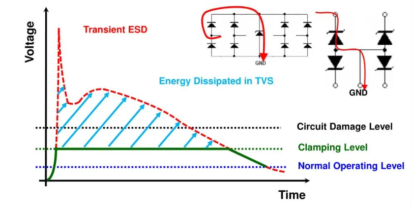
Even the best diode can fail if it sits too far from the connector.Every extra millimeter of trace adds about 1 nanohenry of inductance, and that quickly increases voltage overshoot.Your “5 V clamp” on paper could easily become 12 V in reality if the layout isn’t tight.That’s why TVS arrays must sit as close as possible to the connector pins — ideally within 3 to 5 millimeters, with a wide, short ground via nearby.You can browse TEJTE’s selection of low-capacitance TVS arrays specifically designed for HDMI and USB protection here:Low-cap TVS diode array
How to Align Clamp Voltage to Device Absolute Maximum Ratings
Many engineers think “a 5-volt TVS protects a 5-volt line.”
Not necessarily.Matching clamp voltage to your IC’s absolute maximum rating is one of the most overlooked parts of ESD design.
Avoiding False Conduction
What Capacitance Limit Can HDMI or USB Tolerate?
When you deal with 6–12 Gbps signal rates, capacitance is no longer just a small parasitic — it’s a budget.Every picofarad counts toward your eye opening and jitter margin.You can think of the entire signal path — trace, connector, and protection device — as one continuous RC network. If the total capacitance crosses a certain threshold, your bit edges smear, and equalization inside the PHY can’t save you.
That’s why calculating a capacitance budget before choosing your ESD protection diode is critical.
High-Speed Capacitance Budget Calculator
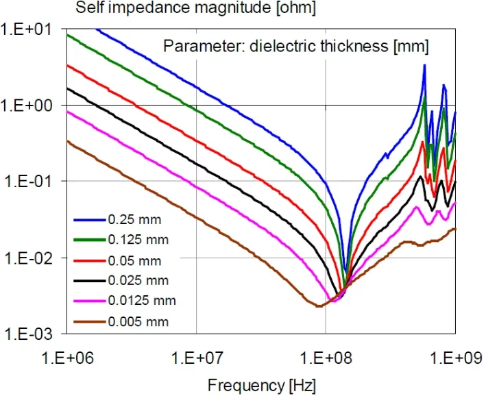
Serving as a visual aid for the input parameters in the “High-Speed Capacitance Budget Calculator” section, this graph illustrates how dielectric thickness affects the impedance characteristics of transmission lines at high frequencies. It helps engineers understand that thinner dielectric layers, while enabling compact layouts, can lead to significant impedance drops, impacting signal integrity. It provides a critical reference for selecting PCB stack-ups and estimating line parasitics.
| Field | Description | Typical Range |
|---|---|---|
| Data rate Rdata | Interface speed (Gbps) | 1 – 12 Gbps |
| Source impedance Zo | 50 Ω for single-ended, 100 Ω for differential | - |
| Trace + connector capacitance | Sum of board and connector capacitance | 0.2 – 0.5 pF |
| TVS diode capacitance | From datasheet, measured at 1 MHz | 0.2 – 1 pF |
| Max rise time tr,max | Calculated from data rate | ≈ 0.35 / Rdata |
Core Equations
- Approximate bandwidth: BW = 0.35 / t_r,max
- Maximum total capacitance: C_total,max = 1 / (2 π × Z0 × BW)
- Capacitance margin: Margin_C = C_total,max − (C_trace+conn + C_TVS)
Decision Rule
- If Margin_C > 0 → The design passes.
- If Margin_C < 0 → You’re over budget. Choose a lower-capacitance diode, move it closer to the connector, or add a small series resistor.
Let’s see an example.
Example:
For a 6 Gbps differential USB 3.0 line (Z0 = 100 Ω):
t_r,max ≈ 0.35 / 6e9 = 58 ps
BW ≈ 6 GHz
C_total,max ≈ 1 / (2 π × 100 × 6e9) ≈ 0.27 pF
If the connector and trace already take 0.15 pF, your TVS can’t exceed roughly 0.12 pF.
That’s why ultra-low-capacitance TVS arrays (< 0.1 pF per line) are mandatory for HDMI 2.1, USB 3.2, and DisplayPort applications.
When You Exceed the Budget: Three Practical Fixes
If you run out of capacitance headroom, you still have a few engineering tricks:
- Pick a lower-C TVS array.
Look for devices under 0.1 pF per channel or use distributed RC networks.
- Move the diode closer to the connector.
Reducing the trace length between the connector and diode minimizes parasitic inductance, which indirectly eases the capacitance load.
- Insert a small series resistor.
Even a 2–3 Ω resistor can reduce reflections and improve eye quality.
This also damps residual ringing caused by ESD diode capacitance.
When you find yourself balancing all three, that’s when ESD protection turns into a high-speed signal design exercise.
Where Should the ESD Diode Sit — Connector Side or Near the IC?
Layout placement defines how effectively your ESD current returns to ground.
Even the best diode will fail if the surge current must travel halfway across the board before reaching the chassis.
The Shortest Loop Wins
The golden rule: place the diode at the connector side, as close to the external pin as possible.
The goal is to shunt the ESD energy to ground before it ever reaches sensitive circuitry.
Use wide copper pours and a ground via within 2–3 mm of the diode pad.
Multiple vias in parallel work better than one thick trace.
Keep the return current loop compact. Each millimeter of added distance adds roughly 1 nH of inductance, which can produce several volts of unwanted overshoot during an ESD pulse.
This is the same reason you often see TVS arrays sitting right next to the HDMI or USB connector shield — it’s not a layout coincidence, it’s survival physics.
Ordering with Common-Mode Chokes, Terminations, and RC Networks
In high-speed lines, several passive elements compete for the same narrow layout space.
Here’s the recommended order from the connector inward:
- Connector → TVS diode array (ESD clamp first)
- Common-mode choke (for EMI suppression)
- ESD ground return via
- Termination resistors or AC-coupling caps
- PHY or SoC pins
The key is to isolate the ESD current path from the signal return path.
Let the ESD energy flow to the board ground without crossing your data loop.
This separation is often what decides whether you pass or fail the IEC 61000-4-2 test.
For a more detailed discussion on port integrity during transient events, check TEJTE’s port integrity under transients article, which covers similar routing rules from a signal-chain perspective.
How to Define “Red Lines” for HDMI Layout Under ESD Stress
High-speed PCB layouts are fragile.
If your HDMI routing violates impedance control or ground referencing, no TVS in the world can save it.
The best approach is to define layout red lines early — the non-negotiable rules your board must respect.
Pair Length, Via Count, and Guard Ground
Here are the practical red lines used in most successful HDMI 2.1 layouts:
- Equal length within differential pairs: keep length mismatch under 5 mils for 6 Gbps links.
- Limit via count: each via adds ~0.3 pF; use at most two per line between connector and PHY.
- Use guard grounds: place ground vias along the differential pair every 2–3 mm to control return current.
- Keep TVS array pads symmetrical: uneven pad layout can unbalance differential impedance.
A simple mistake, like routing one HDMI lane through an extra via, can shift impedance by 5–10 Ω and narrow your eye opening.
Chassis Ground Bonding
When your connector’s shield is isolated from the PCB ground, ESD current must travel through long paths to discharge.
Tie the connector shield to the PCB chassis ground using a low-inductance bridge — copper fingers, spring contacts, or stitching vias.
The goal is to let the surge current flow directly from the connector shell to the board ground plane, avoiding signal traces altogether.
You can visualize it as a “two-step protection”: the TVS array clamps the voltage spike, and the chassis path carries away the energy.
What Capacitance Limit Can HDMI or USB Tolerate?
At high data rates, every picofarad turns into a design decision. Once your signal edges reach tens of picoseconds, that tiny diode capacitance you used to ignore can be the reason your eye diagram collapses. Engineers who have spent a night watching jitter grow on an oscilloscope know exactly what that means.
That’s why high-speed ESD design always begins with one question:“How much total capacitance can this lane afford before it starts to distort?”Instead of guessing, you can treat it like a budget — a sum shared among the trace, connector, and your chosen TVS diode.
Breaking Down the Budget Step by Step
Here’s a simple way to visualize it:
- Trace and connector: they already take part of the budget — typically 0.2 to 0.5 pF per line.
- Protection diode: adds its own portion (often 0.2–1 pF depending on part).
- Allowed total: depends on the interface speed and impedance.
When the sum exceeds what the link can tolerate, the PHY starts fighting reflections, and your link margin disappears.
That’s where the High-Speed Capacitance Budget Calculator helps.
High-Speed Capacitance Budget Calculator
| Parameter | Description | Typical Range |
|---|---|---|
| Data rate Rdata | Interface speed (Gbps) | 1 – 12 Gbps |
| Source impedance Zo | 50 Ω for single-ended, 100 Ω for differential | - |
| Trace + connector capacitance | Sum of board and connector capacitance | 0.2 – 0.5 pF |
| TVS diode capacitance | From datasheet, measured at 1 MHz | 0.2 – 1 pF |
| Max rise time tr,max | Calculated from data rate | ≈ 0.35 / Rdata |
Core math behind it
- Bandwidth: BW = 0.35 / t_r,max
- Allowed total capacitance: C_total,max = 1 / (2π × Z0 × BW)
- Remaining margin: Margin_C = C_total,max − (C_trace+conn + C_TVS)
If the margin is positive, you’re fine.
If it goes negative, it’s time to rethink the design — lower the diode’s capacitance, move it closer to the connector, or add a tiny series resistor to absorb ringing.
Example
Let’s run numbers for a 6-Gbps USB 3.0 differential pair (100-Ω system).
The rise time works out to roughly 58 ps, giving a bandwidth of 6 GHz.
That means the total capacitance must stay below about 0.27 pF.
If the connector and trace already consume 0.15 pF, your ESD diode can’t exceed roughly 0.12 pF.
That’s tight — and exactly why low-capacitance TVS arrays (under 0.1 pF per line) exist.
When the Budget Doesn’t Fit
So what if you’ve already built the prototype, and the eye diagram still looks compressed?
You’ve got three practical levers to pull:
- Switch to an ultra-low-C TVS array.
Look for arrays rated below 0.1 pF per channel — some reach 0.05 pF.
- Bring the diode closer to the connector.
Every extra trace length adds inductance, and that interacts with capacitance to distort the waveform.
- Add a very small resistor in series.
Even 2 Ω of resistance can calm reflections and slightly stretch rise times in a good way.
Sometimes all three are necessary — and that’s normal. ESD design for multi-gigabit lines isn’t about one big fix; it’s about stacking several small ones until the waveform behaves.
Where Should the ESD Diode Sit — Connector or IC Side?
Placement is where most “mystery failures” begin.
I’ve seen otherwise perfect designs fail ESD testing simply because the protection device was a centimeter too far from the port. The physics are simple: ESD current always takes the shortest path to ground. If you make that path long, it will find another — through your chip.
Shortest Loop Rule
Always, always place the ESD protection diode next to the connector. The shorter the discharge loop, the lower the overshoot. Keep the ground return via within 2–3 mm of the diode pad, and if space allows, use two vias instead of one. Think of that diode as a lightning rod — it must catch the strike before the current wanders across your board. Each extra millimeter adds roughly 1 nH of inductance, which can create several volts of unwanted overshoot during an IEC pulse.
That’s why the TVS diode array should sit right beside the connector pins or shield, not halfway between the connector and the PHY.
The Sequence That Actually Works
If your layout also includes common-mode chokes, terminations, or RC filters, their order matters more than most realize.
Here’s the typical arrangement that passes ESD tests most reliably:
- Connector → TVS diode array (first line of defense)
- Common-mode choke (for EMI cleanup)
- Ground return vias
- Termination resistors or AC-coupling caps
- PHY or SoC inputs
The trick is to separate the ESD current loop from the signal return loop. Let the surge energy flow straight to ground without detouring through the data path. That’s the difference between a passing and a failing IEC 61000-4-2 report.
For a broader perspective on how transient events affect entire signal chains, check TEJTE’s port integrity under transients article — it shows how 50-Ω chains behave when struck by fast surges.
Defining “Red Lines” for HDMI Layout Under ESD Stress
Once you step into 6 Gbps and beyond, PCB layout stops being artwork and starts being physics.
If your HDMI differential pairs are unbalanced or poorly referenced to ground, no diode can fix what the copper broke.
That’s why experienced teams set “red lines” — simple layout rules that no one is allowed to violate.
The Unwritten HDMI Rules That Actually Matter
- Keep each differential pair length-matched within 5 mils.
- Avoid unnecessary vias — each one adds about 0.3 pF. Two per line is the hard limit.
- Place guard grounds (stitching vias) every 2–3 mm along the pair to control return current.
- Keep the pads for your TVS array symmetric, so differential impedance doesn’t shift.
When one line sneaks through an extra via, expect the impedance to shift by 5–10 Ω — enough to pinch your eye height by 30 %. A quick TDR check on the board will show the ripple instantly.
Chassis Bonding and Return Path
Here’s a classic trap: the HDMI shield is mechanically grounded but electrically floating. During an ESD strike, that isolation forces current to travel through long detours before discharging — exactly where you don’t want it. The fix is simple but often skipped: bond the connector shell to your board ground through low-inductance bridges, copper fingers, or spring clips.
This lets the surge current dump straight into the chassis instead of wandering across your differential lines. You can picture it as a two-stage protection flow: first the TVS diode clamps the spike, then the chassis path carries the energy away.
How to Plan IEC 61000-4-2 and 61000-4-5 Compliance by Port
Passing IEC compliance tests is not a guessing game. It’s about understanding where the energy flows and how your board handles it.
The two main standards you’ll encounter — IEC 61000-4-2 (electrostatic discharge) and IEC 61000-4-5 (surge immunity) — test entirely different failure modes.
Many designs fail not because the diode was weak, but because the verification plan never mapped the actual discharge path.
Building a Real Test Matrix
Positioned before the “Map the Discharge Path Before Testing” subsection in the chapter “How to Plan IEC Compliance by Port,” this image serves as an educational illustration. It clearly depicts the ideal shortest, lowest-impedance discharge path, visually explaining the physics behind layout rules such as “placing the TVS close to the connector” and “using a wide, short ground connection.” It is a key visual for understanding the core concept of ESD protection layout.
| Port | Test Type | Contact / Air | Voltage Level | Expected Path |
|---|---|---|---|---|
| HDMI | IEC 61000-4-2 | Contact | ±8 kV | Through TVS → GND near connector |
| USB 3.2 | IEC 61000-4-2 | Contact & Air | ±8 kV / ±15 kV | Through TVS → chassis ground |
| DC Input | IEC 61000-4-5 | Surge | ±1 kV | Through power TVS → power ground |
| Ethernet | IEC 61000-4-2 | Contact | ±6 kV | Through TVS + CM choke → chassis |
Map the Discharge Path Before Testing
Before sending a prototype to the lab, trace the ESD current path on the PCB. Literally draw it with a marker if needed.
The shortest loop should start at the connector pin, go through your ESD protection diode, and reach a ground via or copper plane in under 5 mm.
Every extra centimeter of that path increases the voltage spike at your IC by several volts.
For surge testing under IEC 61000-4-5, remember that pulse duration lasts hundreds of microseconds — much longer than the nanosecond-scale ESD event.
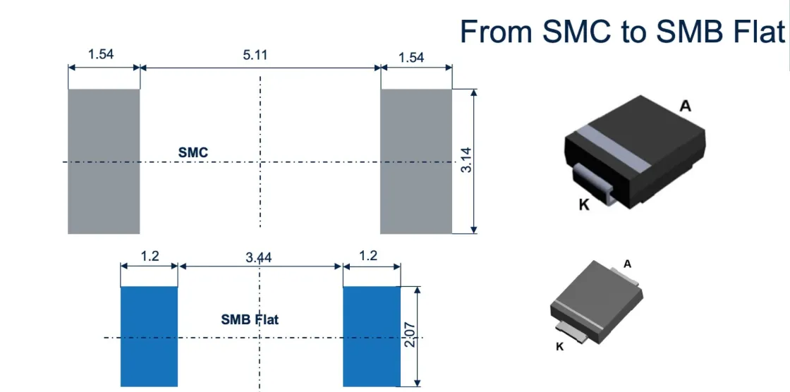
That’s why power input protection typically uses TVS diodes in SMC or SMB packages, while signal ports rely on small ESD arrays optimized for low capacitance.
You can read more on this transition from surge to signal protection in TEJTE’s related article RC snubber vs surge clamp, which explains how surge control moves from passive RC damping to fast silicon clamps.
Should You Include a “Latest News and Updates” Section?
What’s Worth Mentioning
Here’s what typically adds value for your readers or team:
- New low-capacitance TVS series below 0.05 pF, often replacing older 0.2 pF arrays.
- Updated IEC 61000 calibration specs, particularly for discharge waveform tolerances.
- Chipset-driven design notes, where PHY vendors publish exact TVS recommendations for compliance (common for USB4 and HDMI 2.1).
A concise paragraph with 2–3 of these items keeps your article fresh for search engines and genuinely useful for practicing engineers.
Just remember — don’t scatter these notes throughout the post. Put them all here, once, near the end, so your main discussion remains focused.
FAQ — Common Questions About ESD Protection Diodes
1. Should I pick a unidirectional or bidirectional ESD diode for USB or HDMI?
2. What TVS capacitance is “too high” for a 6–12 Gbps lane?
For USB 3.2 and HDMI 2.1, the total capacitance per line — including trace, connector, and diode — must stay below roughly 0.25–0.3 pF.
If your diode adds more than half that, the link will likely fail compliance testing. Always check the manufacturer’s test frequency: capacitance tends to rise at lower bias voltages.
3. Is a TVS array always better than discrete diodes on differential pairs?
Yes, in nearly all high-speed applications. Arrays keep channel matching tight and share a single ground return, which minimizes skew and loop area.
Discrete diodes may still work for low-speed or single-ended lines, but they make routing harder and increase parasitic variation.
4. Where exactly should the ESD diode sit — near the connector or the SoC?
5. Can I fix an eye-diagram failure by moving the TVS instead of changing parts?
Final Thoughts
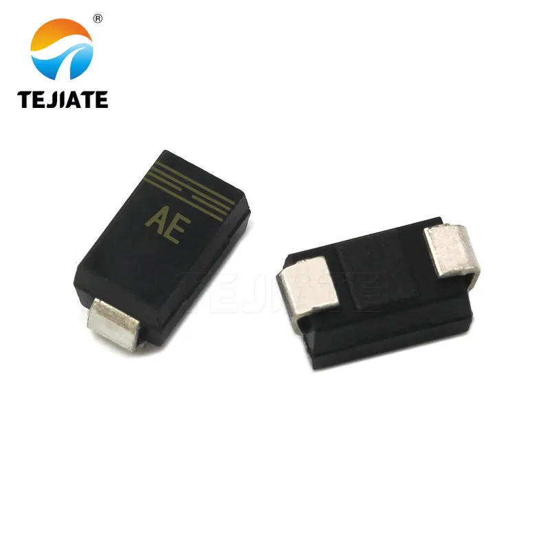
This image serves as a visual element or call-to-action (CTA) graphic at the end of the article. It shows the typical application placement and package forms of the low-capacitance TVS arrays discussed in the article (specifically TEJTE brand products) on an actual PCB. It connects theoretical design with physical components, enhances the article's professionalism and credibility, and provides a visual reference for potential component selection.
Bonfon Office Building, Longgang District, Shenzhen City, Guangdong Province, China

A China-based OEM/ODM RF communications supplier
Table of Contents
Owning your OEM/ODM/Private Label for Electronic Devices andComponents is now easier than ever.
