5V to 12V Boost Converter Design in Practice
Dec 20,2025
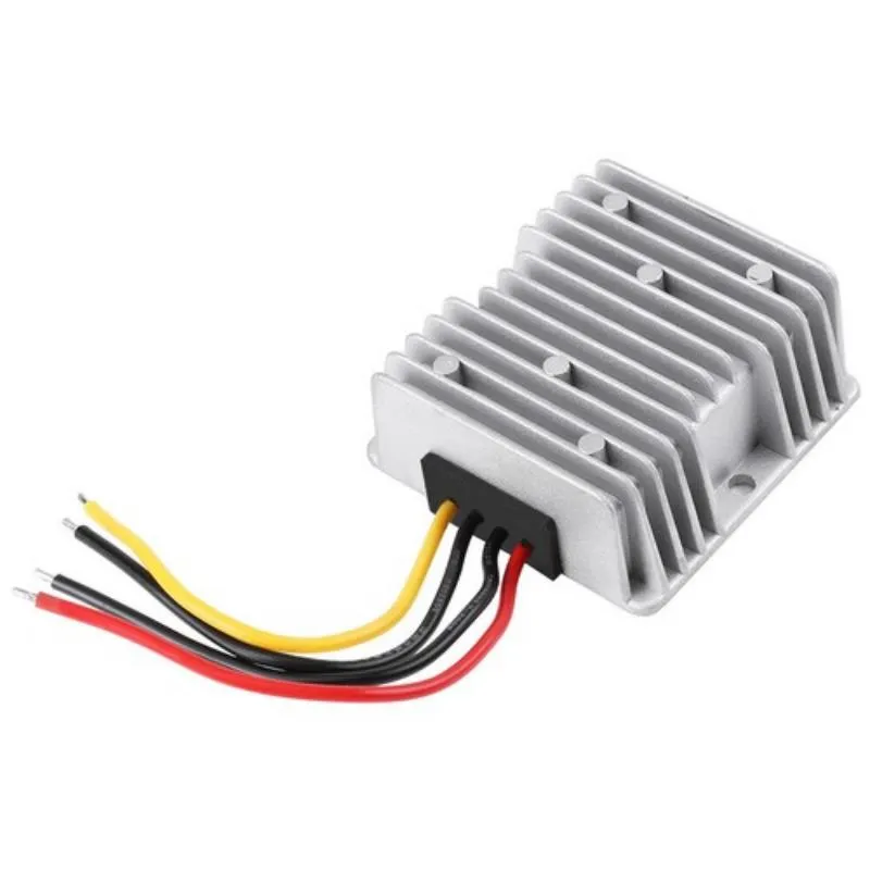
This scene-setting image serves as the opening visual anchor for the article, aiming to immediately establish its practical nature. It visually presents the real challenges engineers face—the waveform ripple and noise visible on the oscilloscope represent the trade-offs rarely warned about in datasheets. The image implies that the subsequent content will address how to solve these practical issues.
Designing a 5V to 12V boost converter sounds straightforward until you build one and watch the waveform ripple across your scope. Real boards expose trade-offs that datasheets rarely warn about — efficiency, thermal margin, and part sourcing. From the veteran MC34063 to today’s integrated synchronous ICs, the path is full of judgment calls that decide whether your converter runs cool or cooks itself.
This practical guide walks through the same steps used by TEJTE engineers when turning a sketch into production-ready hardware — topology, calculation, component selection, layout, and quick validation. If you’ve read our companion article 12V to 5V Buck Converter Design in Practice (anchor: buck vs boost trade-offs), this one flips the direction and exposes the different stress points you’ll face when the current flows the other way.
Which boost topology and controller fit a 5V to 12V goal?
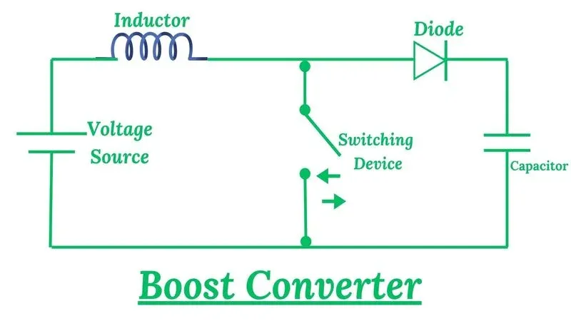
This schematic is the technical foundation for understanding the entire design guide. It clearly deconstructs the core architecture of the boost circuit, translating the abstract concept of “step-up” into specific component interactions. The labeled components (inductor, diode, switch) are the very focus of subsequent chapters on parameter calculation, selection, and layout optimization.
Compare classic controllers vs modern switching regulators
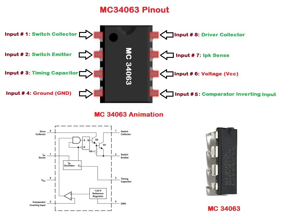
This comparison chart visualizes the path of technological iteration. The left side represents the durable but efficiency-limited classic solution (MC34063), while the right side represents the efficient, highly integrated modern solution. It helps readers make rational controller choices early in a project based on efficiency requirements, thermal budget, and design complexity, echoing the article’s point about “judgment calls that decide whether your converter runs cool or cooks itself.”
The MC34063/MC34063A family refuses to die — and for good reason. They’re rugged, cheap, and sold in nearly every component market worldwide. Yet their 1.25 V switch saturation and external transistor losses limit efficiency to the mid-80 % range.
Modern switching regulators, by contrast, like TI’s TPS61088 or Analog Devices’ LT1302, integrate low-Rds(on) MOSFETs and deliver 90–95 % efficiency even at moderate loads. They also include soft-start, current limiting, and thermal shutdown.
(For a deeper comparison of controller families and their current limits, see our internal reference MC34063 DC-DC Guide: Buck, Boost & Inverting, anchored as MC34063 limits & calculator.)
Define output power, duty-cycle range, and thermal headroom
Let’s anchor the math. Suppose you need 12 V @ 0.2 A output — about 2.4 W. With 5 V input and 85 % efficiency:
[ I_{IN} = \frac{V_{OUT} × I_{OUT}}{η × V_{IN}} ≈ \frac{12×0.2}{0.85×5} ≈ 0.565 A ]
At 0.3 A output, expect roughly 0.85 A input. That single number drives inductor size, diode stress, and switch rating.
For a first-order duty-cycle estimate:
[ D ≈ 1 – \frac{V_{IN} – V_{SAT}}{V_{OUT} + V_F} ]
If the switch drops 0.5 V and your Schottky diode 0.3 V, then ( D ≈ 1 − (5 − 0.5)/(12 + 0.3) ≈ 0.55 ).
A 55 % duty-cycle leaves breathing room for transient spikes.
How do you compute duty cycle, inductor ripple, and switch peak?
Derive D, ΔIL, and I_SW,pk for 5 V to 12 V across VIN(min/max)
At VIN = 4.5 V (brownout corner) and 12 V output, the duty can climb toward 60 %. Assume a switching frequency ( f_{sw} = 100 kHz ) and target ≈ 40 % inductor ripple.
[ L = \frac{V_{IN} × D}{ΔI_L × f_{sw}}, \quad
I_{SW,pk} ≈ \frac{V_{OUT} × I_{OUT}}{η × (V_{IN} – V_{SAT})} + \frac{ΔI_L}{2} ]
These set the foundation for component stress and ripple estimation.
5V to 12V Boost Quick Calculator
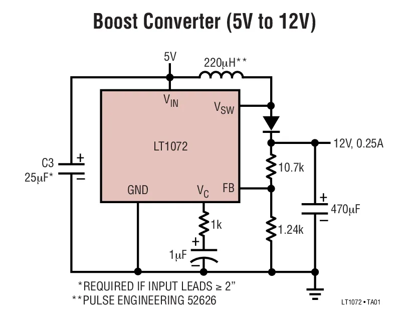
This interface screenshot reinforces the “practical tool” attribute of the article. It packages the complex mathematical formulas from earlier sections into a user-friendly interactive tool, lowering the barrier to design. It aims to attract readers to use TEJTE’s online resources, applying the guide’s theory directly to their own projects, facilitating the transition from “reading” to “designing.”
| Input Parameters | Symbol / Typical Value | Formula / Role |
|---|---|---|
| Minimum input voltage | Vin(min) = 4.5 V | Defines duty-cycle max |
| Output voltage | Vout = 12 V | Fixed target |
| Output current | Iout = 0.2-0.3 A | Design load |
| Switching freq. | fSW = 100 kHz | Sets ripple |
| Inductor ripple | ΔIL = 30-40 % of IL | Trade-off size vs loss |
| Diode drop | VF = 0.3 V | Schottky selection |
| Switch sat. voltage | Vsat = 0.5 V | Controller / MOSFET dependent |
| Efficiency (guess) | η = 0.85 | Start for iteration |
| Cout ESR | ESR = 0.1 Ω | Ripple estimate |
Core Equations
- Duty Cycle
[ D ≈ 1 – \frac{V_{IN} – V_{SAT}}{V_{OUT} + V_F} ]
- Inductance
[ L ≈ \frac{V_{IN} × D}{ΔI_L × f_{sw}} ]
- Switch Peak Current
[ I_{SW,pk} ≈ \frac{V_{OUT} × I_{OUT}}{η × (V_{IN} – V_{SAT})} + \frac{ΔI_L}{2} ]
- Diode Current
[ I_{D,avg} ≈ \frac{V_{OUT} × I_{OUT}}{η × (V_{OUT} + V_F)}, \quad I_{D,pk} ≈ I_{SW,pk} ]
- Output Ripple
[ ΔV_{OUT} ≈ ΔI_L × ESR + \frac{I_{OUT} × D}{C_{OUT} × f_{sw}} ]
- MC34063 Current Sense
[ R_{SC} ≈ \frac{0.3 V}{I_{pk,limit}} ]
(These are reformulated from the boost basics reference for educational use.)
Example 1: 5V to 12V @ 0.2A (light load)
- D ≈ 0.55
- IL(avg) ≈ 0.56 A
- ΔIL ≈ 0.22 A (40 %)
- L ≈ 125 µH
- ISW,pk ≈ 0.67 A
- Diode: 1 A / 20 V (SS14 or MBR120)
- Inductor: 150 µH, Isat ≥ 0.8 A, DCR ≤ 0.25 Ω
Observation: Runs cool, ~84 % efficiency. Ideal for small IoT or logic rails needing 12 V sensors.
Example 2: 5V to 12V @ 0.3A (thermal edge)
- D ≈ 0.56
- IL(avg) ≈ 0.85 A
- ΔIL ≈ 0.34 A
- L ≈ 82 µH
- ISW,pk ≈ 1.02 A
- Diode: 2 A / 20 V (SS24 or MBRS120)
- Inductor: 100 µH, Isat ≥ 1.3 A, DCR ≤ 0.18 Ω
Observation: Hotter surface (~25 °C rise). Dropping diode VF or using a synchronous IC boosts efficiency to ~89 %.
Estimate diode/inductor currents and efficiency bounds before BOM
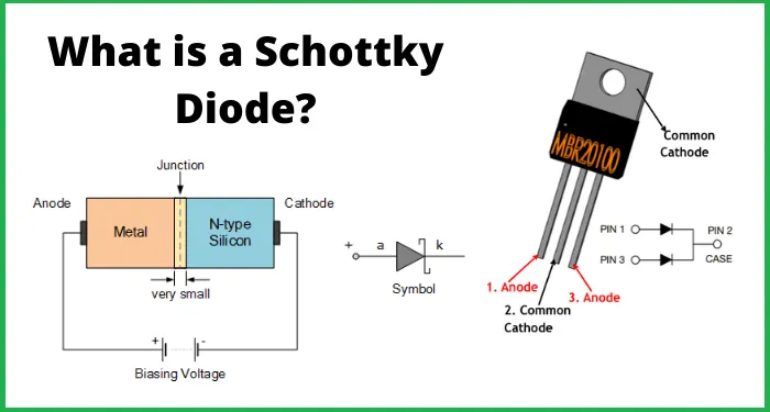
This schematic provides a technical deep-dive for the “Select the Schottky diode” section. It goes beyond a simple parameter table, explaining from a physical level why Schottky diodes are the preferred choice for boost converters (low VF, fast trr). The package information shown also directly relates to subsequent discussions on thermal management and layout, helping readers understand the practical impact of component form on performance.
Real efficiency comes from resistive losses:
[ η ≈ \frac{V_{OUT} × I_{OUT}}{V_{OUT} × I_{OUT} + I_{SW}^2 × R_{ON} + I_{D,avg} × V_F + I_L^2 × DCR} ]
In practice, inductor DCR and diode VF dominate. Spending an extra few cents on low-loss components often saves more heat than a bigger heatsink.
Pro tip: If the converter overheats near 0.3 A, check the diode’s forward voltage and inductor’s DCR before redesigning. They quietly burn more watts than the controller itself.
Select the inductor and Schottky diode without guesswork
Inductor selection: L, Isat, DCR, copper loss vs ripple target
Start with the target inductance computed earlier. But that’s only the opening move — not the final decision. In real builds, saturation current (Isat) and DC resistance (DCR) decide how well the converter performs under heat.
When your calculated ripple current ΔIL is 0.3 A, always ensure Isat ≥ IL(avg) + ΔIL/2, typically adding a 20–30% safety margin.
Low DCR keeps conduction losses small, improving efficiency and lowering board temperature.
| Design Goal | Recommended Range | Why It Matters |
|---|---|---|
| L value | 80 – 150 μH | Controls ripple and transient response |
| Isat | ≥ 1.3 × ISW,pk | Prevents magnetic saturation |
| DCR | ≤ 0.25 Ω | Reduces I²R losses |
| Core type | Ferrite shielded | Limits EMI and acoustic noise |
Diode selection: VF, IF(avg/peak), IR, trr, and thermal rise
Every switching cycle, the diode bears the brunt of the current. The Schottky diode is the default choice because its forward voltage drop (VF) is low—typically 0.25–0.35 V—and reverse recovery time (trr) nearly zero.
When choosing, confirm:
- IF(avg) ≥ Iout × (Vout / Vin)
- IF(pk) ≥ ISW,pk
- VR ≥ 1.5 × Vout (for safety)
- VF as low as possible
- IR (leakage) low enough not to waste standby current
For 5 to 12 V designs up to 0.3 A output, the SS14 (1 A/40 V) or SS24 (2 A/40 V) diodes are time-tested favorites.
Higher-current builds or temperature-sensitive layouts may switch to MBRS120 or MBRS220 series.
(For background on diode structure and trade-offs, refer to low-VF diodes on Wikipedia.)
Tip: A diode running hotter than your inductor signals VF too high or poor thermal dissipation. Consider larger packages (SMA to SMB) or move to synchronous regulation.
What goes into a short, order-ready BOM?
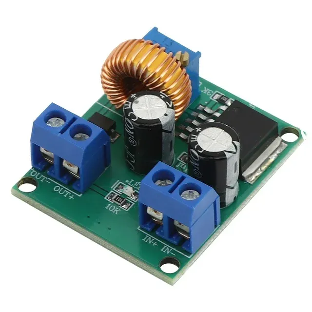
This physical image is a visual representation of the theoretical BOM list. It translates abstract component designators and specifications into a concrete circuit board, providing readers with a reliable layout reference template. The relative placement of components, pad sizes, and trace widths in the image imply design considerations for optimizing thermal and electrical performance, serving as a hub connecting the “component selection” and “layout” chapters.
Controller + L + D + Cin/Cout + sensing/comp parts
| Category | Example Components | Specs / Notes |
|---|---|---|
| Controller IC | MC34063A / TPS61088 / LT1302 | DIP-8 or DFN, available globally |
| Inductor | 100 μH, 1.3 A Isat, ≤ 0.25 Ω DCR | Shielded ferrite preferred |
| Diode | SS24 or MBRS120 | ≥ 2 A / 20 V rating |
| Cin (input cap) | 100 μF / 16 V Low-ESR electrolytic | Bypasses high di/dt loops |
| Cout (output cap) | 220 μF / 25 V Low-ESR | Controls output ripple |
| RSC (sense) | RSC ≈ 0.3 V / Ipk,limit | Current-limit tuning |
| Compensation | 10 kΩ + 10 nF (typical) | Loop stability |
| Optional Snubber | 100 Ω + 330 pF | Damps ringing across switch/diode node |
Second sources and footprint notes for quick procurement
When your factory runs on a tight deadline, cross-reference footprints across two vendors. For inductors, the 744771110 (Würth Elektronik) and CDRH104R-101 (Sumida) share nearly identical pad geometry. Diodes like SS24 and MBR240 can substitute without PCB change.
This simple discipline turns your BOM into a ready-for-purchase document, shortening your prototype-to-production cycle by weeks.
What layout rules keep EMI and ringing under control?
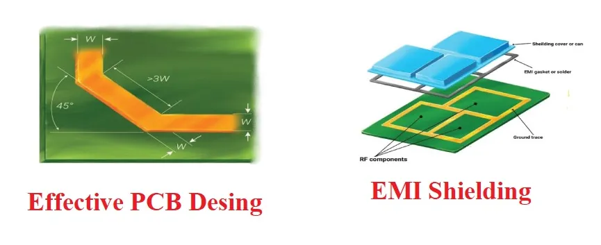
This schematic is a crucial visual guide for controlling noise and ringing. It abstracts and emphasizes the core principles of good layout: minimizing the area of the high-frequency switching loop, correct placement of input/output capacitors for decoupling, and using a star ground point. The arrows and annotations directly correspond to specific advice in the text, such as “shrink the high-di/dt loop” and “add a snubber,” turning textual descriptions into actionable layout steps.
Shrink the high-di/dt loop, place Cin/Cout tight, add snubber if needed
Keep the input capacitor (Cin) physically adjacent to the controller’s switch node and ground. Every extra millimeter of trace adds inductance that rings during switching edges.
- Route the switch–diode–inductor loop short and fat.
- Use a star-ground returning to a single point under the IC.
- Place Cout close to the diode and load return path.
If ringing still appears, add a snubber: start with 100 Ω + 330 pF across the diode. Adjust values empirically by observing waveform damping on a high-bandwidth scope.
(For more on loop design principles, our 12 V to 5 V Buck Converter Guide explains shared EMI strategies for both topologies.)
Grounding, probe pads, and ripple/efficiency measurement points
Testing often fails not because the converter is bad, but because there’s nowhere clean to probe. Add dedicated pads for:
- VIN test (after input filter)
- SW node (for ringing measurement)
- VOUT ripple (Kelvin pair)
- Ground sense (near controller pin)
Use twisted wires or coax probes to minimize injected noise. Always ground your oscilloscope probe tip within 1 cm of the measurement pad.
Can you validate the prototype quickly and safely?
Line/load sweeps, ripple spectrum, and peak-current verification
Run VIN sweeps from 4.5 V to 5.5 V while holding a 12 V output load. Track efficiency and ripple at each step. If the converter enters discontinuous mode too early, revisit your inductor or compensation network.
Measure ripple spectrum using FFT mode on a digital scope. For EMI pre-compliance, the 100 kHz fundamental should sit at least 20 dB below your target spec.
Verify ISW,pk under worst load with a current probe—compare with your calculation from the Quick Calculator.
(Our internal MC34063 limits & calculator article provides sample test setups for these checks.)
Thermal scan under worst-case VIN(min) and 12 V @ target load
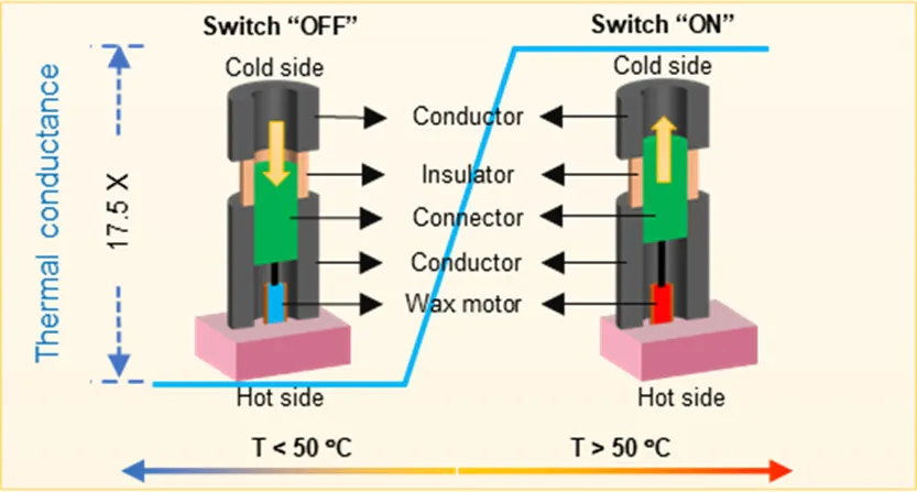
This image provides a powerful visualization of the abstract concept of “thermal management.” Instead of just listing temperature numbers, it uses a comparative scenario to let readers immediately see the vast difference in thermal performance between good and poor designs. It supports the article’s discussion on “full-load burn-in testing” and “hotspots should not exceed 85°C,” and implies that solving overheating issues requires attention to both materials (thermal conductivity) and physical structure (hot-side path).
Run a full-load burn-in at VIN = 4.5 V for 10 minutes. Record surface temperatures of the switch, diode, and inductor with an IR camera or thermocouple.
Expect hotspots near 65–75 °C under open air. If you see anything beyond 85 °C, that’s your cue to upgrade the diode or inductor.
When efficiency feels “off,” don’t chase numbers blindly—map where the heat actually goes. Hot copper tells the truth faster than equations.
When should you avoid this approach and switch regulators?
Very low noise/EMI, high efficiency, or tiny footprint constraints
If your application drives sensitive analog or RF circuits, like preamps or transceivers, switching noise may still leak through even with tight layout and LC filtering. In those cases, a low-noise switching regulator or hybrid module with internal shielding is the safer bet.
Likewise, when you need >90% efficiency at 0.3 A or more, discrete boost topologies hit their thermal ceiling. Integrated synchronous boost ICs eliminate the Schottky losses entirely, replacing the diode with a controlled MOSFET.
And when space is scarce — say, in compact IoT devices or handheld instruments — modern regulators like the TPS61291 or MAX1709 fit everything into a 3×3 mm footprint with minimal external components.
Alternatives: synchronous boost modules or higher-frequency ICs
Off-the-shelf synchronous boost modules are no longer luxury parts. They often come pretested for EMC and thermal performance, with efficiencies above 92%.
At frequencies above 1 MHz, newer ICs reduce inductor size dramatically while maintaining stable transient behavior.
A few typical replacements for the 5 to 12 V class include:
| IC / Module | Key Specs | Why It Helps |
|---|---|---|
| TPS61291 (TI) | 1 MHz, 95 % typ. efficiency | Integrated FETs, low ripple |
| LT1302 (ADI) | 600 kHz, 2 A switch | Handles 5 to 12 V easily |
| MP3429 (MPS) | 1.2 MHz, 2 A sync boost | High integration, tiny footprint |
| XL6009 (XL Semi) | 400 kHz, 4 A external switch | Budget alternative, easy sourcing |
These ICs outperform discrete MC34063 circuits both electrically and mechanically, though they cost slightly more. For designs scaling beyond 1 W, that trade-off pays back in stability and lifetime.
Internal link suggestion: See TEJTE’s 12V to 5V Buck Converter Design in Practice for a complementary down-conversion guide — a useful contrast when evaluating buck vs boost trade-offs.
Frequently Asked Questions (FAQ)
1. Why does my boost converter overheat at light load even though calculations look fine?
Light-load overheating often signals poor switching mode transition. Many older controllers (including MC34063) enter discontinuous or pulse-skipping modes that raise switching losses when output current drops.
Check gate drive waveforms; if the transistor never fully saturates, efficiency will dive even at low current.
2. What ESR range on Cout keeps ripple acceptable without stability issues?
Aim for 0.05–0.2 Ω ESR at your switching frequency. Too low (like MLCC-only outputs) can destabilize older feedback loops. Too high, and output ripple grows beyond 100 mVpp.
Electrolytics with parallel ceramics strike a good balance between stability and low noise.
3. Can MC34063 reliably deliver 12 V from 5 V, or should I move to a modern switching regulator?
Yes—MC34063 can deliver up to 12 V at 0.2–0.25 A comfortably with correct component sizing. Beyond that, efficiency drops below 80%, and thermal stress rises sharply.
If you need more current, compactness, or better EMI compliance, move to a modern switching regulator such as the LT1302 or TPS61088.
For deeper design data, visit TEJTE’s MC34063 DC-DC Guide: Buck, Boost & Inverting.
4. How do I probe the high-di/dt loop to confirm the layout is actually good?
Use short ground leads (under 1 cm) on your oscilloscope probe and measure at the diode–switch node. If ringing exceeds 10–15% of VIN, loop inductance is excessive.
Adding a small RC snubber (100 Ω + 330 pF) usually cleans it up. Never rely on long alligator leads—they mislead more than they measure.
5. What fails first under brownout or transients, and how do I set current limit safely?
Under brownout (VIN < 4.5 V), switch current rises fastest, not the diode current. Set the sense resistor ( R_{SC} ) for 20–25% margin below your transistor’s absolute maximum current.
Remember: current spikes, not average current, decide survival. Always test at VIN(min) before shipping your design.
Industry Pulse & Closing Insight
In the sub-5 W power range, the humble boost converter remains a go-to choice thanks to component availability and cost. Many TEJTE customers still rely on MC34063-based 5 to 12 V circuits for test rigs, routers, and IoT devices where board area isn’t premium.
Yet, synchronous ICs are steadily gaining ground wherever compliance, miniaturization, and long-term efficiency matter. The real trick lies not in chasing “perfect parts,” but in matching the converter’s thermal, EMI, and sourcing realities to your application.
For further reading and practical contrast, see:
- 12V to 5V Buck Converter Design in Practice — explore buck vs boost trade-offs
- MC34063 DC-DC Guide: Buck, Boost & Inverting — learn about controller behavior & limitations
- Boost converter basics — theoretical background
- Schottky diode fundamentals — why low VF matters
Final Word
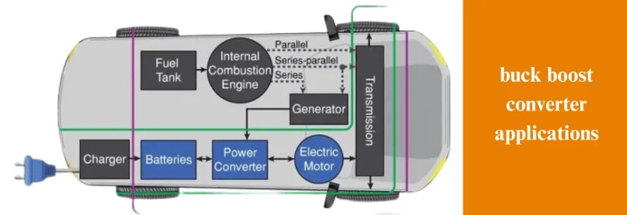
This application scenario image serves as the conclusion of the article, placing all the preceding technical discussions (topology, calculation, selection, layout) within the context of a real product ecosystem. It answers the fundamental question, “What can I use this circuit for?” By showcasing the role of the boost module in specific applications like IoT devices and motor drivers, it reinforces the practical value of the design guide and inspires readers to apply it to their own projects.
Whether you’re using a legacy controller or a cutting-edge IC, designing a 5V to 12V boost converter teaches one core lesson: every milliamp counts. Proper sizing, clean layout, and verified thermal margins make the difference between “works on the bench” and “runs for years.”
If you’re integrating DC-DC designs into a broader RF or embedded system, visit tejte.com — your one-stop source for RF connectors, power modules, and custom cable assemblies engineered to move ideas from schematic to field hardware fast.
Bonfon Office Building, Longgang District, Shenzhen City, Guangdong Province, China

A China-based OEM/ODM RF communications supplier
Table of Contents
Owning your OEM/ODM/Private Label for Electronic Devices andComponents is now easier than ever.
