12V MOSFET Guide: BUK9Y29-40E,115 for Automotive & Power Design
Nov 12,2025
Preface

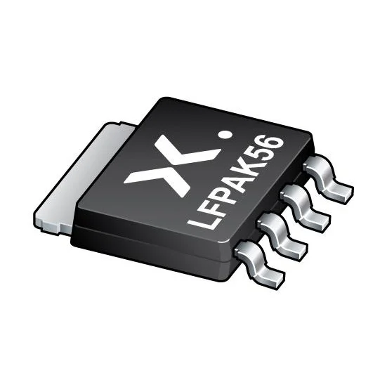
Based on the document's preface, this diagram demonstrates the core application value of Nexperia TrenchMOS™ series MOSFETs in 12V systems, highlighting their ability to achieve low loss and high reliability in space-constrained designs
Every engineer working around 12 V systems eventually faces the same decision: choosing a MOSFET that balances low loss, reliability, and cost — all without needing a gate driver the size of a matchbox.
Nexperia’s BUK9Y29-40E,115, part of the TrenchMOS™ line, has quietly become one of those go-to parts for switching solenoids, DC motors, and automotive lighting rails.
It’s compact, runs cool when mounted right, and has proven its worth in dozens of 12 V applications we’ve seen on the bench.
Can this 12V MOSFET meet automotive-grade reliability targets?

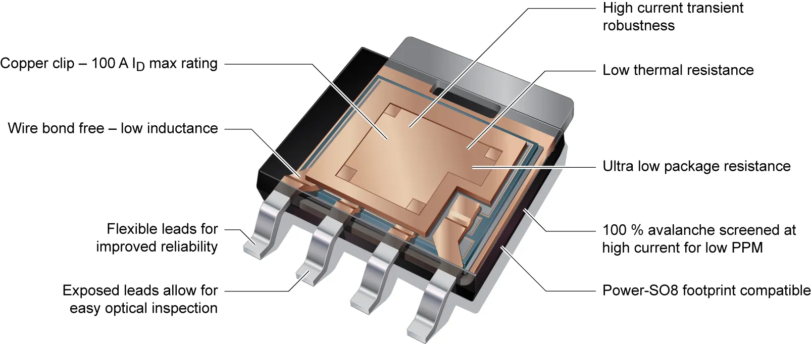
This diagram clearly shows the physical characteristics of the LFPAK56 package, including copper clip technology, lead-free bonding design and exposed thermal pad, providing excellent thermal performance and low package resistance for 12V high-current applications
In the automotive world, qualification is everything. The BUK9Y29-40E,115 isn’t just another 40-volt FET — it’s a fully AEC-Q101 qualified device, built to survive harsh under-hood conditions.
It operates from –55 °C to 175 °C (Tj) and handles 25 A continuous drain current (Tc) with 37 W power dissipation, giving more than enough margin for 12 V rails that can swing toward 40 V during transients.
The part sits inside Nexperia’s TrenchMOS™ family, known for consistent silicon geometry and avalanche-rated cells.
Internal change logs (PCNs) confirm a stable production chain — wafer-fab updates in late 2023, label and packaging revisions in 2024 — which matters when you’re building an automotive PPAP file.
It’s also RoHS3 compliant, REACH-safe, and rated MSL 1, so it stores indefinitely without dry-pack fuss.
If you’re running design comparisons, its LFPAK56 / Power-SO8 package delivers rugged thermal behavior for compact boards.
The base device ID (BUK9Y29) has been around for several generations, a quiet sign of long-term reliability.
You’ll find similar components listed under Semiconductor Devices for 12 V Systems — TEJTE’s technical catalog for automotive MOSFETs and protection elements.
How do you confirm true 5 V logic-level drive on BUK9Y29-40E,115?
Plenty of MOSFETs advertise “logic-level,” but not all behave well at 5 V.
This one does, and the data back it up.
The threshold voltage is just 2.1 V @ 1 mA, so conduction begins early.
At 5 V gate drive, its Rds(on) stays near 29 mΩ (typ.), close to 25 mΩ @ 10 V, proving that the die is optimized for low-voltage enhancement.
Add to that a total gate charge of 5 nC @ 5 V and Ciss ≈ 664 pF @ 25 V, and you get a transistor that an MCU can drive directly — no dedicated gate driver needed in many 12 V load paths.
If you’re using a microcontroller output pin, just place a 10 Ω gate resistor to tame dI/dt and noise.
That setup easily reaches sub-50 ns edge times, clean enough for PWM up to 100 kHz.
A quick logic-drive checklist looks like this:
- Verify Rds(on) vs. Vgs curves in the datasheet (the 5 V trace should flatten early).
- Estimate switching time ≈ Qg / I_driver.
- Keep Vgs within ±10 V, the absolute limit for the LFPAK56 cell.
- Route gate and source returns as a tight pair to reduce loop inductance.
In short, BUK9Y29-40E,115 behaves like a true 5 V MOSFET, not a 10 V part disguised as one.
If you want a deeper dive into drive waveforms and safe-operating-area margining, check the engineering note Logic-Level MOSFET in 12 V Load Design & SOA Practice on TEJTE’s blog.
Estimate losses in minutes with the quick model?
Before you start routing copper, it helps to know how much heat this MOSFET will really make.
Here’s a compact calculator model based on real parameters from BUK9Y29-40E,115.
| Parameter | Symbol / Formula | Typical Value | Remarks |
|---|---|---|---|
| Drain current | I_load | 8 A | Continuous DC load |
| Duty ratio | D | 0.8 | 80 % on-time |
| Switching frequency | Fsw | 50 kHz | Mid-range PWM |
| Gate voltage | Vgs | 5 V | Logic-level |
| Rds(on) | — | 29 mΩ @ 5 V | From datasheet |
| Qg | — | 5 nC @ 5 V | From datasheet |
| Thermal resistance | RθJA | 50 °C/W | LFPAK56 on 2 oz Cu |
| Ambient temperature | Tamb | 55 °C | Under-hood |
| Temperature coefficient | α | 0.004 / °C | Silicon slope |
Equations
[ P_{cond} = I_{rms}^2 × R_{ds(on)} × (1 + α·ΔT) ]
[ P_{sw} ≈ Q_g × V_{gs} × F_{sw} ]
[ ΔT_j ≈ (P_{cond} + P_{sw}) × R_{θJA} ]
Example calculation
- (P_{cond} = 8^2 × 0.029 ≈ 1.86 W)
- (P_{sw} = 5 × 10^{-9} × 5 × 50 000 ≈ 1.25 W)
- (P_{total} ≈ 3.11 W)
- (ΔT_j = 3.11 × 50 = 155 °C) → Tj ≈ 210 °C, beyond safe range
Clearly, thermal design dominates here. Expanding copper area or lowering switching frequency cuts junction rise sharply.
You can classify copper zones as:
- Small (S): < 50 mm² → RθJA ≈ 70 °C/W
- Medium (M): ≈ 100 mm² → RθJA ≈ 50 °C/W
- Large (L): > 200 mm² → RθJA ≈ 35 °C/W
Using this quick estimator, you can spot-check whether your layout will stay inside Tj < 175 °C limits.
A digital version of this calculator is being integrated into TEJTE’s 12 V MOSFET Estimator Tool to simplify early-stage thermal checks.
How should you lay out LFPAK56 (Power-SO8) for safe junction temps?

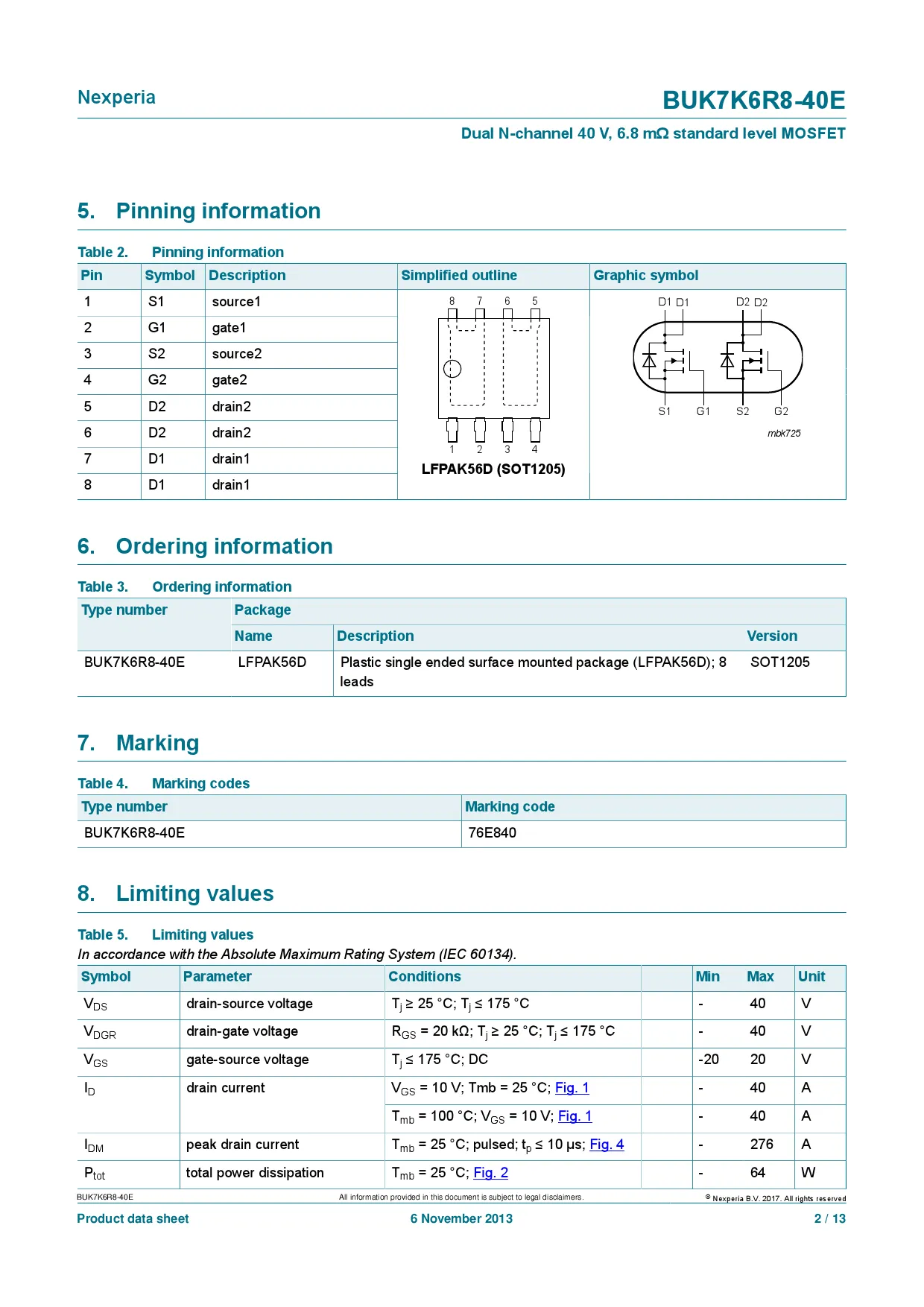
This diagram verifies the true logic-level capability of the MOSFET through key electrical parameters, including 2.1V threshold voltage, 29mΩ on-resistance at 5V drive and 5nC gate charge, proving it can be directly driven by MCUs
Thermal behavior in a 12 V MOSFET often depends less on the silicon and more on the copper beneath it.
The BUK9Y29-40E,115, housed in LFPAK56 (Power-SO8), uses a direct copper clip between die and lead frame.
That clip spreads current evenly and keeps the thermal path short — one reason this package achieves roughly 50 °C/W RθJA on a medium copper pad.
When designing the layout:
- Expose the thermal pad to a wide copper region. Anything above 100 mm² meaningfully lowers junction rise.
- Use a via array — four to eight vias under the pad — to pull heat into inner planes.
- Thicken the copper, ideally 2 oz or more, on both top and inner layers for high-current traces.
- Maintain short, wide drain paths; voltage drop here turns straight into unnecessary loss.
For soldering, keep the stencil aperture around 50–60 % coverage to avoid voids, and confirm that your IR reflow peaks near 250 °C ± 5 °C.
It’s easy to miss that uneven solder voids can double the effective RθJA even when you meet paste thickness specs.
If you’re building compact PCBs for power electronics, check TEJTE’s RF Connector Layout and Mounting Guide ︎ for similar grounding and thermal-spreading practices — those same ideas translate perfectly to hot-running Power-SO8 MOSFETs.
What SOA checks are mandatory for inductive and lamp loads?

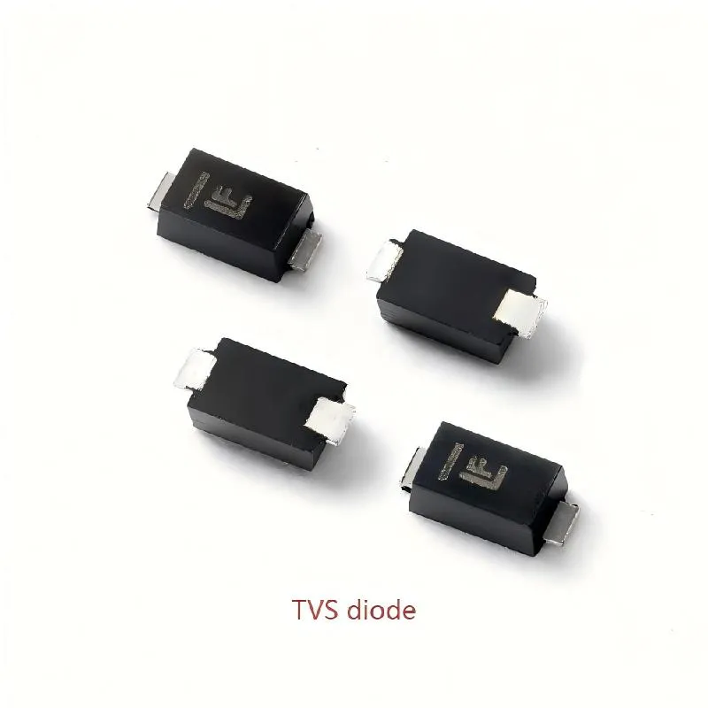
This diagram shows the actual appearance of automotive-grade TVS diodes, which feature fast response characteristics and high energy absorption capability, effectively suppressing transient overvoltage generated when switching inductive loads when placed near the MOSFET drain
Driving inductive or filament loads is where many 12 V MOSFETs fail first — not from steady current but from voltage spikes.
The BUK9Y29-40E,115 is avalanche-rated and tested per AEC-Q101, but you still need to leave guardband.
Key design habits:
- Clamp dI/dt early. Use a TVS diode close to the drain or across the supply.
- Snub the source with a small RC network if ringing persists above 20 MHz.
- Limit repetitive avalanche energy to well under the datasheet EAS; this part’s silicon family handles pulses but not infinite ones.
- Keep the Vds overshoot < 80 % of its 40 V rating. Once you see more, you’re already off the safe-operating-area curve.
On the bench, verify with a differential probe across the drain and source: short bursts should settle within two switching cycles.
A clean trace means you’ve respected the MOSFET’s SOA boundary and won’t burn junction corners.
If you want a deeper look at transient protection, the TEJTE blog article TVS Placement for Solenoids and 12 V Loads ︎ discusses placement, routing, and pulse energy matching — principles that apply directly to the BUK9Y29-40E,115 family.
How do you pick copper area classes without over-design?
Thermal management doesn’t always mean adding metal until it’s heavy; it means sizing smart.
Using the Loss & Temperature Mini-Estimator, you can translate junction targets into Copper Area Classes (S / M / L) that fit your PCB budget.
| Copper Class | Approx. Area | RθJA (typ.) | Notes |
|---|---|---|---|
| S - Small Pad | < 50 mm² | ≈ 70 °C/W | Use only for low-duty control paths |
| M - Medium Pad | ≈ 100 mm² | ≈ 50 °C/W | Typical for 8-10 A continuous load |
| L - Large Pad | > 200 mm² | ≈ 35 °C/W | Recommended for sustained PWM drive above 6 A |
Here’s how the trade-off looks in practice:
- At 25 °C ambient, even a small pad keeps Tj below 120 °C for 5 A loads.
- At 55 °C, you’ll need at least a Medium pad to maintain 20 °C margin to Tj limit.
- At 85 °C, only Large pads or heavier copper maintain reliability without derating.
It’s often more cost-effective to double copper thickness than to stretch board area.
Two-ounce copper cuts thermal resistance by ≈ 25 %, which in many cases equals a whole size jump.
To visualize how layout size and current interact, you can experiment with the estimator inside TEJTE’s 12 V MOSFET Loss & Temperature Tool ︎ — it mirrors the same formulas used throughout this article.
In the end, the right copper class depends on your PWM frequency, ambient band (25 / 55 / 85 °C), and how close your design lives to the 175 °C junction limit.

This diagram explains the necessary Safe Operating Area checks when driving inductive loads like motors and solenoids, including limiting repetitive avalanche energy and maintaining Vds overshoot within safe range to prevent premature device failure
Could Ciss and Qg limit PWM or startup events?
When you push a 12 V MOSFET toward high-frequency PWM, it’s not the drain current that complains first — it’s the gate.
The BUK9Y29-40E,115 has a modest total gate charge (Qg) ≈ 5 nC @ 5 V and an input capacitance Ciss ≈ 664 pF @ 25 V, so it’s friendly to microcontroller drivers.
Still, every system has a crossover point where switching loss overtakes conduction efficiency.
You can estimate that point with a simple thumb rule:
[ P_{sw} ≈ Q_g × V_{gs} × F_{sw} ]
At 5 V drive and 5 nC gate charge, 50 kHz costs about 1.25 W — fine for short bursts but worth attention under continuous load.
As frequency rises, switching loss scales linearly while conduction loss stays flat, so by 100 kHz the balance flips.
That’s why designers often slow down the gate slightly with a series resistor (5 – 15 Ω) or use a small MOSFET driver IC to sharpen transitions.
The extra resistor also reduces dV/dt noise that can couple into nearby sensors — something you’ll notice fast in mixed-signal automotive boards.
For startup events or inrush control, add a soft-gate capacitor (10 – 100 nF) from gate to ground through a resistor divider.
This forms an RC ramp so the MOSFET opens gradually, protecting fuses and avoiding brownouts on secondary rails.
If you’d like to review practical timing and RC shaping examples, TEJTE’s article Logic-Level MOSFET in 12 V Load Design & SOA Practice ︎ expands on gate-drive damping and EMI tuning.
What changed in 2024–2025 that impacts device selection?
The 12 V domain is evolving quietly but steadily. While wide-bandgap devices get headlines, most vehicles and low-voltage systems still rely on advanced silicon MOSFETs.
Nexperia’s 2025 updates emphasize package innovation rather than new voltage classes — the company refined its LFPAK56 and introduced tighter parametric screening across AEC-Q101 batches, reducing lot-to-lot variation.
That’s valuable when your board carries ten identical switches in parallel.
Meanwhile, other semiconductor players have been raising the bar:
- Navitas Semiconductor announced automotive-grade GaN packages in May 2025, targeting 400 V+ systems but hinting at trickle-down benefits for 12 V auxiliaries.
- iDEAL Semiconductor reached its AEC-Q101 milestone in October 2025, showing how smaller foundries are pushing qualification discipline downstream.
- Nexperia also published R&D notes on compact SiC prototypes, though their TrenchMOS™ line remains the mainstream workhorse for 12 V rails.
The bottom line: for 12 V loads, silicon MOSFETs in Power-SO8/LFPAK56 still offer the best blend of cost, footprint, and thermal reliability.
If you track such component shifts, TEJTE’s Semiconductor Devices Hub ︎ summarizes release cycles and qualification updates across brands.
Build a bench-top validation plan in one afternoon?
A quick validation routine doesn’t need fancy automation — just discipline.
Here’s a three-stage plan to qualify any 12 V MOSFET like the BUK9Y29-40E,115 on your lab bench:
1. Static verification
- Measure Rds(on) at ambient, 75 °C, and 125 °C using a four-wire Kelvin jig.
- Record voltage drop at 5 A, 10 A, and 20 A to map thermal rise.
2. Dynamic switching test
- Use a low-side setup with PWM (20 kHz–100 kHz).
- Capture gate-source and drain-source waveforms.
- Compute switching energy: (E_{sw} = ½ × Vds × Id × t_{rise+fall}).
Stay below 80 % of the datasheet’s SOA curve.
3. Thermal observation
- Run at rated load until temperature stabilizes.
- Aim for Tj ≤ 155 °C, leaving ≥ 20 °C margin below the 175 °C limit.
- Use an IR camera or a thermocouple on the drain pad; note any hot spots near the clip edge.
Pass/Fail logic is simple: the device passes if ΔTj < 120 °C at the worst ambient and no waveform overshoot exceeds the 40 V rating.
When all three checks line up, you can sign off on SOA integrity with confidence.
For repeatable test setups and comparison data, TEJTE’s lab notes inside BNC Extension Cable Routing Guide show how signal-integrity testing translates to power-device validation — the measurement discipline is the same.
Where does BUK9Y29-40E,115 fit best in 12 V systems?
Every 12 V MOSFET finds its niche, and this one fits the mid-power bracket beautifully.
Its 25 A Id, 29 mΩ typical Rds(on), and compact LFPAK56 footprint make it ideal for:
- Solenoid drivers in ABS, fuel, or valve control units.
- DC motor controllers for fans and window actuators.
- LED and lighting rails needing fast PWM and compact thermal paths.
- Relay replacement switches where Rds(on) dominates efficiency.
It’s also a natural upgrade path for older DPAK designs when board space or efficiency demands a tighter footprint.
The Power-SO8/LFPAK56 package shares thermal parity with bulkier through-hole parts yet offers fully visible leads for optical inspection — something line operators appreciate during automotive builds.
For reference designs and cross-package comparisons, the TEJTE library at tejte.com/blog includes several application notes linking RF connectors, power switches, and thermal layout concepts into a single design philosophy.
Frequently Asked Questions
Q1. Is a 5 V MCU output enough to drive the BUK9Y29-40E,115 directly?
Yes. The BUK9Y29-40E,115 is a true logic-level 12 V MOSFET, switching fully at 5 V gate drive.
Its Qg ≈ 5 nC and Ciss ≈ 664 pF make it compatible with most MCU pins.
Still, adding a 10 Ω gate resistor helps control EMI and damp ringing at higher PWM frequencies.
Q2. What’s the maximum safe temperature for this MOSFET in continuous 12 V operation?
Its rated junction temperature (Tj max) is 175 °C, but you should design for Tj ≤ 155 °C to maintain margin.
The Mini-Estimator model in this guide shows that copper pad size and airflow dominate temperature control.
Q3. How do I confirm the AEC-Q101 qualification status?
Check the manufacturer’s datasheet or the Nexperia PCN history —
the BUK9Y29-40E,115 has passed full automotive-grade reliability testing,
including temperature cycling, gate bias, and avalanche stress.
Q4. Does this 12 V MOSFET need an external diode for inductive loads?
It includes body-diode protection, but external TVS diodes or RC snubbers are still recommended
when driving motors, solenoids, or lamps.
Proper clamping ensures compliance with SOA and prolongs the MOSFET’s life.
Q5. What PCB layout best suits the LFPAK56 package?
Use a solid copper pad tied to ground or supply plane, with multiple thermal vias directly under the drain pad.
Avoid voids in the solder joint and maintain short, wide traces for current flow.
Following this approach typically yields RθJA ≈ 50 °C/W, sufficient for most 12 V systems.
Q6. What’s a reasonable PWM range for switching applications?
The device operates efficiently up to 100 kHz.
Beyond that, switching loss (Psw ≈ Qg × Vgs × Fsw) increases rapidly.
At 50 kHz, total loss remains around 3 W with a proper copper pad and airflow.
Q7. Where can I find similar 12 V MOSFETs or reference designs?
TEJTE maintains a curated catalog of automotive MOSFETs and semiconductor devices at tejte.com/products/semiconductor-devices-2/ ︎,along with application notes and layout tips on tejte.com/blog ︎.
Bonfon Office Building, Longgang District, Shenzhen City, Guangdong Province, China

A China-based OEM/ODM RF communications supplier
Table of Contents
Owning your OEM/ODM/Private Label for Electronic Devices andComponents is now easier than ever.
