SMP Connector Guide for High-Density RF Boards
Feb 05,2025
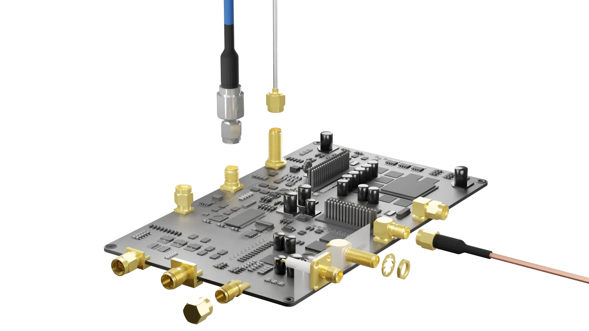
The context for Figure 1 (Page 1) states upfront that RF system failures are often unexpected, and connectors become the "quiet limiter" due to neglect. Therefore, this figure is likely a comparative schematic or infographic. The left side might show a "Dense RF Module" or "Stacked Boards" using traditional connectors (e.g., SMA), where connectors are bulky, spacing is limited, and annotations like "Size Limitation," "Hard to Blind-Mate," or "Becoming Architectural Bottleneck" are present. The right side shows a similar system using SMP Connectors, with connectors being small and densely packed, arrows indicating "Blind-Mate Engagement," "High-Density Placement," and "Preserving Frequency Headroom." This figure aims to visually establish the core value proposition of SMP connectors: they are not a universal interface but an engineering solution specifically for size, density, and manufacturability challenges, thus introducing the need for the in-depth discussion that follows.
RF systems usually don’t fail where engineers expect them to.
When something degrades, the instinct is to look at active devices first—PA compression, LNA noise figure drift, clock leakage, firmware timing. Connectors almost never make that first shortlist.
That blind spot is exactly why interconnect problems survive so long in dense RF hardware.
In compact radio modules, backplanes, and stacked boards, the connector often becomes the quiet limiter. Not because it is “bad,” but because it was chosen late, sized for convenience, or treated as electrically invisible. At low channel counts, that assumption holds. As density increases, it doesn’t.
This is the design space where the SMP connector starts to matter.
SMP is not a universal RF interface. It is not meant for front panels, field technicians, or frequent hand mating. It exists for one job: moving RF signals through very tight mechanical spaces while keeping frequency headroom and enabling blind-mate assembly. If your design never hits those constraints, you may never need it. If it does, SMP quickly stops being optional.
Why should you consider an SMP connector for dense RF boards?
Balancing size, frequency, and channel density
Every RF connector represents a compromise, whether it is acknowledged or not. SMA trades size for robustness. MCX and MMCX trade frequency margin for footprint. None of these trade-offs feel painful until a system scales.
The SMP connector shifts the balance in a different way. It gives up threaded engagement entirely and replaces it with a push-on, snap-style interface that tolerates blind mating. In exchange, it allows connectors to be placed far closer together than SMA ever could, while still supporting frequencies well into the tens of gigahertz.
On paper, many SMP RF connector families advertise 40 GHz capability. In practice, most real boards never operate that high, especially on FR-4. What matters more is that SMP does not become the bottleneck at 6, 12, or even 18 GHz when channel density increases. SMA often does.
Another difference shows up mechanically. SMP systems are designed with bullets and floating interfaces that absorb small misalignments. That flexibility is not about convenience—it is about survival once tolerances stack up across PCB thickness, connector coplanarity, and enclosure machining.
Why SMP starts to win as systems scale
At low channel counts, SMA works fine. It is forgiving, well understood, and easy to debug in the lab. The problem is that SMA does not scale gracefully. Threaded connectors consume board edge. Torque requirements slow assembly. Blind mating is essentially impossible.
As RF systems grow denser—multi-channel radios, phased arrays, modular front ends—the connector stops being a detail and starts shaping the architecture. Designers begin spacing channels around the connector instead of the other way around.
This is usually the moment SMP enters the conversation.
Blind-mate capability changes how boards are assembled and serviced. High-density placement changes how many channels fit in a given volume. Together, those traits enable backplanes and stacked RF modules that would be mechanically fragile—or outright impossible—with threaded connectors.
How should you choose SMP form factors and interface directions?
Board-to-board versus cable-to-board SMP usage
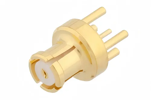
Figure 2 is explicitly titled “图2 Board-to-Board SMP,” and its context (Page 3) details the advantages of direct board-to-board SMP connections (minimized loss, predictable phase) and their stringent prerequisites (tightly controlled stack height, disciplined mechanical design). Therefore, this figure should be a technical schematic or cross-section clearly showing two parallel PCBs directly mated via SMP connectors. The image might highlight key details: the precise Stack Height, the strict alignment at the connector interface, and possibly an annotation like “Low-Loss Path.” Additionally, dashed lines or arrows might indicate this rigid connection’s high sensitivity to tolerance stack-up, where any minor misalignment translates directly into mechanical stress. This figure visually presents an “ideal yet demanding” form of SMP application.
One of the first misconceptions about SMP is that it must always be board-to-board. In reality, many successful designs use a mix of rigid and flexible SMP interfaces.
Direct board-to-board SMP connections are ideal when stack height is well controlled and repeatability matters. They minimize loss, reduce interfaces, and keep phase behavior predictable. The downside is that they demand discipline in mechanical design. Small errors show up quickly.
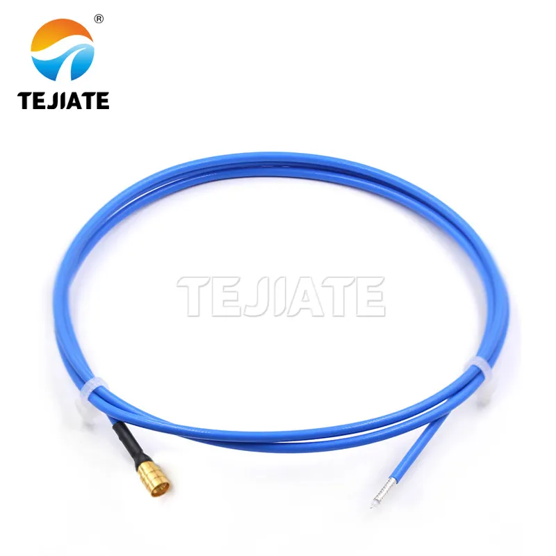
Figure 3 is titled “图3 SMP Cable,” and its context (Page 4) immediately follows Figure 2, introducing short SMP cable assemblies as an alternative. The text notes that cable assemblies introduce extra interfaces but provide valuable mechanical tolerance. Therefore, this figure should be a physical image or schematic of an SMP cable assembly. It would clearly show a flexible coaxial cable (possibly RG316) terminated with SMP connectors (male or female) on both ends. The image might demonstrate its “flexibility” by showing the cable in a bent state, and could annotate key advantages like “Absorbs Misalignment,” “Simplifies Routing in Cramped Spaces,” or “Useful for Early Prototypes.” This figure directly contrasts with the rigid connection in Figure 2, presenting a practical solution for SMP in the face of real-world mechanical uncertainties.
Short SMP cable assemblies fill the gaps where that discipline is hard to maintain. They add flexibility, tolerate slight offsets, and simplify routing in crowded enclosures. Yes, they introduce extra interfaces, but in many layouts the mechanical relief is worth the trade.
In early prototypes, cable-based SMP links are especially useful. Once the mechanical envelope stabilizes, some of those links can be replaced with direct connections. Designs that lock into rigid SMP interfaces too early often regret it.
Straight, right-angle, and floating SMP designs
Orientation choices with SMP are not cosmetic. Straight SMP connectors give the cleanest electrical transition but leave almost no room for stack-up error. Right-angle versions save vertical space but complicate the RF launch and grounding.
Floating SMP connectors solve a different problem entirely. They allow limited movement during mating, absorbing misalignment that would otherwise stress solder joints or deform contacts. In blind-mate systems, floating designs are often the difference between a connector that works in the lab and one that survives production.
From a reliability standpoint, floating SMP designs tend to age better, especially in systems exposed to vibration or thermal cycling.
When does an SSMA connector still make sense?
The SSMA connector sits awkwardly between SMA and SMP. It keeps a threaded interface while reducing size, which makes it attractive in legacy designs where mating force and vibration resistance matter.
What SSMA does not offer is density or blind-mate capability. Threads impose spacing limits and slow assembly. For new designs pushing channel count or modularity, SMP usually outpaces SSMA quickly.
Engineers often arrive at this conclusion after revisiting SMA trade-offs in detail, especially when comparing internal versus external RF interfaces. Discussions like those in SMA Connector Selection for RF Cables and Antennas are often part of that decision process.
How should SMP connector decisions show up in the schematic and BOM?
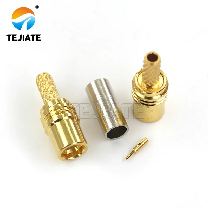
Figure 4 is titled “图4 SMP Male,” and its context (Pages 6-7) delves into how SMP connectors can easily cause confusion in schematics and Bills of Materials (BOMs), emphasizing the need to specify the connector’s role (e.g., male, female, floating bullet) clearly. Therefore, this figure is undoubtedly a close-up of an SMP male connector, likely in the form of a product photo or detailed engineering drawing. The image would clearly show key features: the Center Pin/Piston, the Outer Conductor/Shell, and the interface mechanism for snap-on mating. It might include dimension callouts or a cross-sectional view to emphasize its compactness. The core purpose of this figure is to provide a clear visual reference for “SMP Male,” helping engineers specify parts accurately in documentation and preventing mismatches during assembly.
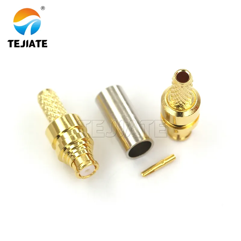
Figure 5 is titled “图5 SMP Female,” and its context is closely linked to Figure 4, further explaining that an SMP interface may involve a plug, jack, and floating bullet, and any ambiguity in documentation causes issues. Therefore, this figure is a close-up of an SMP female connector, serving as the mating counterpart to the male in Figure 4. The image would highlight the female connector’s features: the Center Receptacle for receiving the male pin, the Outer Conductor/Shell, and the corresponding snap mechanism. By juxtaposing or contrasting Figures 4 and 5, the article aims to give readers an intuitive understanding of the gender pairing in SMP connectors and reinforce a key message: in SMP systems, “male” and “female” cannot be inferred solely from part numbers; they must be explicitly labeled in design documentation, otherwise production chaos ensues.
Most SMP-related problems don’t start on the PCB.
They start much earlier, usually when the schematic is considered “done” and the connector is treated as a solved detail.
SMP does not behave like SMA in documentation. There is no simple male–female pairing that everyone intuitively understands. A functional SMP interface may involve a plug on one board, a jack on another, and a floating bullet in between. Electrically, this is straightforward. Organizationally, it is fragile.
If the schematic symbol or BOM line item does not make that relationship explicit, mistakes propagate quietly. Assembly teams pick the wrong mating part. Test fixtures don’t line up. Someone notices only after an RF path goes dead.
This is why experienced teams label SMP parts by role, not just by part number. It feels redundant at first. Later, it saves hours.
Why multiple SMP variants amplify risk
Dense RF boards often mix SMP styles without much ceremony. Straight connectors here, right-angle ones there, floating mounts in a few critical spots. Electrically, this is manageable. Logistically, it raises the stakes.
Every additional SMP variant increases the chance of a feeder error, a placement mix-up, or a mismatched mate. In low-volume builds, engineers catch these issues by inspection. In higher volumes, they slip through.
Teams that have been burned by this tend to standardize aggressively. Not because it improves RF performance, but because it stabilizes everything around it.
Where does SMP cable actually make sense?
Cable choices are often mechanical, not RF-driven

Figure 6 is explicitly titled “图6 SMP Male to SMA Female Cable,” and its context (Pages 9-10) states that few RF labs natively speak SMP; test equipment and engineers expect SMA, making SMP-to-SMA adapters essential. The text emphasizes that the trouble is not using adapters—it’s pretending they won’t be needed and not designing space for them. Therefore, this figure should be a physical image of an SMP-to-SMA cable assembly. It would clearly show both ends: one end with an SMP male connector (for the device’s SMP port) and the other with an SMA female connector (for test cables or instruments). The image might annotate its function as a “Test Access Point” or “Fault Isolation Tool.” This figure visualizes a critical practical consideration: regardless of how advanced the internal design is, interfacing with the external standard test environment must be planned ahead; adapters are part of the workflow, not an afterthought
On paper, it’s easy to compare cable loss curves and frequency ratings. In compact systems, those numbers rarely drive the final decision. What matters is how the cable behaves when the enclosure closes.
Short SMP cable assemblies are often used not because rigid board-to-board links are electrically inferior, but because the mechanical reality is messy. Shields, heat spreaders, nearby connectors—all of these force compromises.
RG316 shows up in these assemblies for predictable reasons. It bends without protest, survives temperature swings, and keeps impedance under control at short lengths. RG178 trades robustness for size. Semi-rigid coax improves repeatability but resists last-minute layout changes.
Most designs don’t choose a cable type once. They converge on it after a few revisions.
Consistency matters more than optimization
One of the easiest ways to introduce unexplained variation is to mix cable types across channels without a strong reason. Electrically, the differences may look small. System-level behavior rarely agrees.
Engineers often revisit cable trade-offs after reviewing broader coax behavior in context, especially when balancing flexibility against loss and temperature limits. References like RG316 coaxial cable loss and temperature characteristics are often used at that stage, not to optimize, but to justify consistency.
When does an SMP to SMA adapter belong in the design?
Adapters are part of the workflow, whether planned or not
Very few RF labs speak SMP natively. Test equipment expects SMA. Engineers expect quick access. This mismatch is where the SMP to SMA adapter quietly becomes essential.
What causes trouble is not using adapters—it’s pretending they won’t be needed. Designs that leave no physical or mechanical room for adapters force awkward workarounds later: stressed cables, repeated mating, improvised fixtures.
Treating adapters as a temporary interface, rather than an afterthought, makes early bring-up calmer and faster.
Adapters as fault-isolation tools
Adapters also earn their keep long after validation. In field debugging, converting an internal SMP node to SMA allows engineers to break a signal chain cleanly. This kind of isolation is standard practice in modular RF systems, even if it is rarely documented.
The important constraint is restraint. Adapters are diagnostic tools, not permanent RF elements. Leaving them in the final signal path usually creates more problems than it solves.
Why do SMP connector pads and launches need extra care?
Small geometry, small margin
SMP connectors are unforgiving simply because they are small. There is less copper to work with, less room for ground stitching, and less tolerance for asymmetry. What SMA tolerates, SMP often exposes.
Most performance issues attributed to the SMP RF connector itself turn out to be launch problems. Pad size is off. Ground return is interrupted. A via stub resonates right where it shouldn’t.
This is not a connector flaw. It is a scaling issue.
Engineers who are new to SMP often benefit from stepping back and reviewing general RF connector behavior—how impedance continuity and reference planes interact—before locking a footprint. Broad overviews such as coaxial RF connector fundamentals help frame these constraints without tying them to a specific vendor or layout.
Edge versus mid-board placement is not neutral
Edge-mounted SMP connectors naturally couple to ground planes and simplify return paths. Mid-board placements demand more discipline: tighter via spacing, controlled clearances, and better symmetry.
Neither approach is wrong. Mixing them casually is.
Practical checklist: SMP pad and transition review
| Item | Check |
|---|---|
| Connector family | SMP / SSMP / SMPM |
| Target impedance | 50 Ω |
| Stackup reference | Verified |
| Dielectric thickness | Matches calculation |
| Trace width | Calculated, not guessed |
| Pad dimensions | Match datasheet |
| Ground vias | Sufficient and symmetric |
| Via pitch | ≤ λ/20 at operating band |
| Copper clearance | ≥ 1.5 × trace width |
| Simulated S11 | Reviewed |
| Status | Accept / Rework |
None of this is exotic. The failure mode is skipping it because the connector “should handle it.”
It won’t.
Why schematic clarity matters more than it looks
SMP-based designs magnify ambiguity. A vague connector symbol or an unclear note in the schematic can ripple into layout assumptions, assembly instructions, and test procedures.
Teams that treat schematic clarity as part of RF integrity—not just documentation—tend to catch problems earlier. Others discover them when the system is already assembled.
Many engineers cross-check their assumptions against general RF interface principles from standards bodies such as the IEC’s RF connector framework, not to replace simulation, but to avoid violating fundamentals while chasing density.
How do you route RF traces into an SMP connector on multilayer boards?
Microstrip or stripline: the decision is rarely theoretical
On paper, the choice between microstrip and stripline looks straightforward. Microstrip is easy to tune and inspect. Stripline offers better shielding and isolation. In dense RF boards, the decision is usually driven by everything except theory.
If the SMP connector sits on an outer layer, microstrip often wins by default. The transition is simpler, the launch geometry is visible, and tuning during early revisions is faster. The downside is exposure—surface routing is more sensitive to nearby metal, covers, and fasteners.
Stripline becomes attractive when internal routing dominates or when EMI containment matters. The trade-off shows up at the launch. Bringing a stripline cleanly into an SMP connector requires disciplined via transitions and careful reference-plane management. Sloppy transitions here erase the benefits of stripline entirely.
Many mature designs use both. Internal stripline routing transitions to microstrip near the connector, not because it is elegant, but because it is controllable.
Why via stubs start to matter above single-digit GHz
At low frequencies, via stubs are easy to ignore. At higher frequencies, they stop being theoretical. A stub that looks harmless at 3 GHz can introduce a sharp resonance at 12 or 15 GHz.
SMP launches amplify this effect because everything is compact. There is less electrical length to hide discontinuities. Back-drilling, blind vias, or carefully controlled via depths become relevant earlier than they would with larger connectors.
The mistake is assuming every SMP interface needs aggressive via mitigation. Many do not. The right question is whether the operating band overlaps with the stub resonance. If it does, the problem will show up eventually—often after layout feels “finished.”
What layout problems only appear during system integration?
Mechanical stress masquerading as RF noise
One of the more frustrating SMP failure modes is intermittent RF behavior caused by mechanical stress. The connector mates cleanly on the bench. Measurements look stable. After integration, channels drift or drop intermittently.
The root cause is often contact pressure changing under load. Slight misalignment, enclosure stress, or board flex alters how the SMP interfaces engage. Electrically, this looks like noise or mismatch. Mechanically, it is a tolerance issue.
Floating SMP designs reduce this risk, but they do not eliminate it. Mechanical review around SMP locations matters just as much as RF simulation.
Vibration and thermal cycling expose weak assumptions
Thermal expansion and vibration are excellent lie detectors. They reveal which SMP interfaces rely on perfect alignment and which ones tolerate reality.
Boards that pass room-temperature testing can fail after a few thermal cycles if stack height errors accumulate. Vibration can loosen marginal contacts without ever causing visible damage.
This is why reliability planning for SMP connectors usually goes beyond datasheet mating cycles. Engineers think in terms of what moves and what pushes back.
How do you manage mechanical and thermal reliability of SMP RF connectors?
Mating cycles and retention force are not academic numbers
SMP connectors are not designed for frequent user mating. Their rated mating cycles are typically lower than SMA, and that matters during development and test.
Repeated mating during debug wears contacts faster than many teams expect. This becomes visible when a connector that behaved perfectly in early prototypes starts acting “touchy” later in the project.
Good teams track mating cycles informally. Bad ones assume connectors are immortal.
Retention force also deserves attention. Floating SMP interfaces trade holding force for alignment tolerance. That trade is usually worth it, but it means the surrounding mechanical structure must do more work to keep boards seated.
Stack-up tolerance is a system problem
No single component controls stack height. PCB thickness, connector coplanarity, standoffs, and enclosure machining all contribute. SMP connectors sit at the mercy of that entire chain.
Designs that explicitly manage this—by allowing float, adding alignment features, or defining hard mechanical datums—age better. Designs that rely on nominal dimensions rarely do.
This is not unique to SMP, but SMP makes the consequences obvious.
How should SMP connectors be tested and qualified?
Production screening: catch gross defects, not perfection
In production, SMP testing is about filtering obvious failures, not proving perfection. Low-current contact resistance checks catch bad mating. Spot S-parameter or TDR checks identify outliers.
Trying to fully characterize every channel is usually counterproductive. The goal is consistency, not lab-grade data.
Using SMP to SMA adapters during test and service
Adapters resurface here. During production test, SMP to SMA adapters allow quick access to internal nodes without custom fixtures. In service, they help isolate faults without tearing down the entire system.
Their usefulness is proportional to how early they were planned for. Designs that leave physical space and mechanical clearance for adapters are easier to support over time.
What does long-term maintenance look like for SMP-based systems?
Visual inspection still matters
SMP connectors fail quietly. Plating wear, contamination, or slight deformation may not show up electrically at first. Periodic visual inspection catches issues before they become intermittent faults.
This is especially relevant in systems that are opened occasionally for upgrades or repair.
Monitoring through behavior, not just measurements
Long-term issues often appear as trends rather than hard failures: increasing sensitivity to temperature, changes in return loss after reassembly, or channels that behave differently after maintenance.
Engineers who treat these as signals—not noise—tend to identify SMP-related issues earlier.
Where does the SMP connector actually fit in modern RF systems?
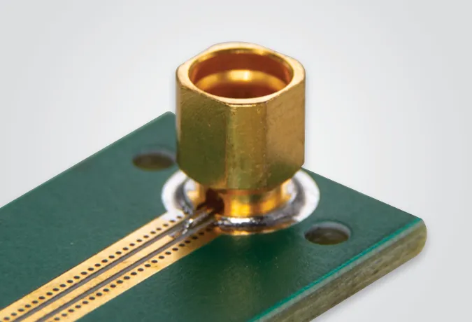
Figure 7 is simply titled “图7,” and its context (Pages 17-18) concludes by comparing SMP with smaller SMPM/SMPS variants and emphasizing that SMP connectors are key enablers for modular RF systems (like phased array tiles, replaceable front ends) because they support dense, repeatable, blind-mate interconnects. Therefore, this figure should be a system-level application schematic. It might depict a modular RF subsystem composed of multiple “RF Tiles” or “Front-End Modules” interconnected via board-to-board SMP connectors and short SMP cables, all mounted within a Backplane or Chassis. The image would highlight the design concepts of blind-mate engagement, high channel density, and ease of upgrade/maintenance. This figure aims to elevate all the preceding technical discussions about SMP to the level of system value and business impact (service life, upgrade paths), providing a fitting conclusion to the article.
SMP versus SMPM and SMPS in practice
As frequencies climb and modules shrink, smaller interfaces like SMPM and SMPS gain attention. They serve a purpose, especially in mmWave front ends. What they lack is mechanical robustness and forgiveness.
SMP remains common in intermediate-frequency and RF interconnects where density matters but survivability still counts. It occupies a middle ground that many systems still need.
Modular RF systems depend on predictable interconnects
Modern RF architectures increasingly rely on modular tiles and replaceable front ends. SMP connectors enable this by supporting dense, repeatable, blind-mate interconnects without excessive manual handling.
That modularity is not just a convenience. In aerospace, satellite, and infrastructure systems, it directly affects service life and upgrade paths.
Engineers often ground these decisions in established RF connector families and standards, cross-checking against general interconnect principles from bodies such as the IEC RF connector classifications or broad summaries like coaxial RF connector families to ensure nothing fundamental is overlooked.
Closing note
SMP connectors do not fix sloppy RF design. They expose it.
Used deliberately, they unlock architectures that threaded connectors cannot support at scale. Used casually, they create subtle problems that surface late and cost time.
The difference is rarely the connector itself. It is how early—and how honestly—it is treated as part of the system.
Bonfon Office Building, Longgang District, Shenzhen City, Guangdong Province, China

A China-based OEM/ODM RF communications supplier
Table of Contents
Owning your OEM/ODM/Private Label for Electronic Devices andComponents is now easier than ever.
