TVS Diode for CAN: PESD2CAN,215 Selection & Layout
Nov 2,2025
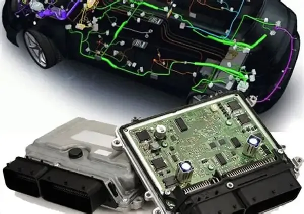
aims to resonate with design engineers by visually highlighting the importance of component lifecycle management, setting the stage for the document's discussion on the status, risks, and alternatives to the PESD2CAN,215.
Should you still design in PESD2CAN,215 or migrate now?
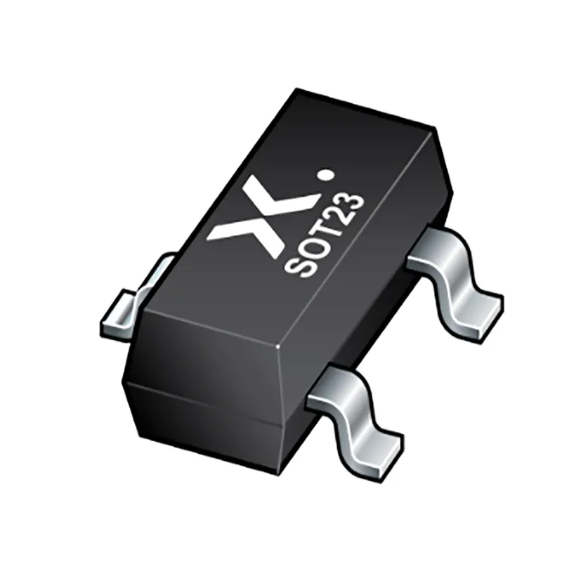
When you design a CAN or CAN-FD interface, one small diode quietly decides your compliance margin — the TVS diode. For years, engineers have trusted Nexperia’s PESD2CAN,215, a compact SOT-23 dual-line transient voltage suppressor built specifically for automotive CAN nodes. Yet, like many reliable workhorses, it now carries a note you can’t ignore: “Not Recommended for New Design (NRND).”
That NRND status doesn’t mean failure — it means lifecycle caution. Distributors like Mouser and Farnell still stock it in tape-and-reel (TR/CT) packaging, but Nexperia’s own product status flags the part as nearing its retirement phase. If you’re locking a new PCB layout for 2025 or later, you’ll need to think about supply continuity. Once production inventory drains, sourcing becomes inconsistent, and automotive PPAP compliance might become difficult.
Still, why do so many engineers hold onto it? The PESD2CAN,215 offers a practical mix of numbers that just work:
- Reverse stand-off voltage (VRWM): 24 V
- Breakdown voltage (VBR): ≥ 26.2 V
- Clamping voltage (VC): ~41 V at 5 A (8/20 µs pulse)
- Capacitance (Cp): ~25 pF @ 1 MHz
- AEC-Q101 qualified, with a –55 °C to +150 °C operating range.
That balance—low enough capacitance for standard CAN and CAN-FD up to 2 Mbps, high enough surge rating for ±30 kV contact discharge (IEC 61000-4-2)—has kept this diode relevant.
Lifecycle & Risk Note
Nexperia’s latest PCNs confirm several packaging updates (SOT-23 tape material, label format, and resin hardener changes between 2020–2024). These don’t alter performance but indicate an aging product line being phased for next-gen alternatives. In short, it’s still safe for sustaining projects, but for new designs, plan your second source early — more on that later in this guide.
Internal reference: for readers exploring other protection parts, see TEJTE’s ESD protection collection — it provides guidance on automotive-grade layout and surge compliance.
Which TVS diode specs actually matter for CAN/CAN-FD?
Mapping the key specs
| Parameter | PESD2CAN,215 Typical | Design Impact |
|---|---|---|
| VRWM (Reverse Stand-Off Voltage) | 24 V | Must exceed normal bus common-mode (±12 V typical, 24 V max). |
| VBR (Breakdown Voltage) | ≥ 26.2 V | Ensures quick response to ±30 kV contact ESD pulses. |
| VC (Clamping Voltage @ 5 A, 8/20 μs) | ≤ 41 V | Must stay below CAN transceiver's absolute max rating (often ±58 V). |
| Cp (Capacitance @ 1 MHz) | 25 pF | Limits data rate: acceptable for classic CAN, borderline for >5 Mbps CAN-FD. |
| AEC-Q101 Qualified | Yes | Required for automotive compliance. |
| Operating Range | -55 °C ~ +150 °C | Guarantees stability across ECU temperature swing. |
These four — VRWM, VC, Cp, and qualification — determine whether a diode is actually compatible with your CAN transceiver’s absolute max voltage and data-rate margin.
In short:
- Too low VRWM, and you’ll clamp normal signals.
- Too high VC, and you’ll burn the transceiver pins.
- Too high Cp, and your eye diagram collapses at 8–10 Mbps.
Regulatory Perspective
PESD2CAN,215 meets AEC-Q101 standards and passes IEC 61000-4-2 (up to ±30 kV contact). These two marks are the “language” of automotive EMC. AEC-Q101 ensures lot-to-lot reliability under temperature cycling, while IEC 61000-4-2 defines actual immunity to human-body ESD events.
For CAN systems operating on both 12 V and 24 V vehicles, a 24 V TVS diode comfortably covers both rails because the signal lines are differential and float near ground potential. You only need to make sure it’s not used on the power supply rail—that’s a different beast (load-dump protection).
If you want to cross-reference parts, distributors like Mouser Electronics list equivalents with similar 41 V clamp and 25 pF capacitance, such as Bourns CDSOT23-T24CAN-Q and ST ESDCAN24-2BLY. We’ll evaluate those replacements later.
Where should the CAN TVS sit—connector, transceiver, or both?
This is the single most common question on design forums — and the most misunderstood.
If you’ve ever seen a CAN transceiver fail during ESD testing, odds are the diode was physically too far from the connector. Every extra millimeter of copper trace adds inductance, and at nanosecond timescales, inductance turns into voltage overshoot:
ΔV ≈ L × di/dt
1. The connector-side rule
Place the TVS diode as close to the CAN connector pins (CANH, CANL) as possible — ideally within 3–5 mm. The goal is to route the surge energy to chassis ground before it reaches the transceiver.
A simple layout heuristic:
- Keep the trace between the connector pin and the TVS shorter than 5 mm.
- Use two or more ground vias right beside the diode pad to minimize equivalent series inductance (ESL).
- Avoid routing under or around large copper gaps; continuous return paths matter more than via count.
2. Interaction with termination and chokes
Many CAN networks include a split termination (2 × 60 Ω + 4.7 nF to ground) and a common-mode choke (CMC) right behind the connector. The TVS should sit ahead of the CMC — that way, it clamps surge energy before it couples through the choke and saturates it.
If you put the TVS after the choke, the energy sees a higher impedance path and might still arc across the transceiver. In contrast, placing it upfront ensures both lines see a symmetric clamp path.
At TEJTE, our own RF assemblies and ESD-rated connectors follow the same grounding philosophy — short paths, wide returns, and minimal via length. For a detailed look at physical examples, you can browse our connector layout practices.
How do you verify clamp safety for your transceiver?
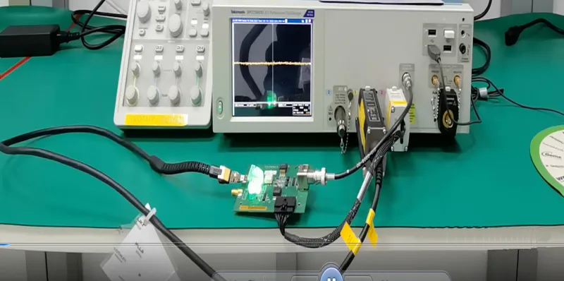
It combines theoretical calculation (VC < V_ABS_MAX) with a practical lab validation scenario, emphasizing the importance of physical measurement in design.
Quick sanity check
Here’s a practical clamp check engineers use in real-world validation:
[ VC_{max} < V_{ABS_MAX(CANH/L)} ]
For the PESD2CAN,215,
- VC(max) = 41 V @ 5 A (8/20 µs pulse)
- Transceiver ABS MAX ≈ ±58 V
Result: safe. Even under full surge, the diode will protect without forward-biasing or overstressing the transceiver input cells.
Still, lab verification tells the full story. You can validate this using an IEC 61000-4-2 ESD gun (330 Ω/150 pF network) fired directly at the connector shield, while probing the CANH/CANL lines with a 500 MHz oscilloscope. Watch the voltage at the transceiver pins: the goal is to see a smooth clamp around 35–40 V without ringing above the absolute limit.
For engineers who also deal with RF or high-speed buses, the same principle applies: keep the return path tight and verify VC under realistic pulse energy, not just datasheet conditions.
For additional guidance on surge validation, see TEJTE’s IEC 61000-4-2 testing checklist, which details pulse shaping, contact discharge setup, and common lab pitfalls.
Can PESD2CAN,215 drop-in to CAN-FD or do you need lower Cp?
Here’s where things get tricky. The original PESD2CAN,215 was designed in an era when classical CAN topped out at 1 Mbps. Modern CAN-FD can reach 5–8 Mbps, sometimes even 10 Mbps in diagnostics mode. At those speeds, line capacitance (Cp) matters far more than surge rating.
The PESD2CAN,215’s 25 pF capacitance is fine for 1 Mbps, borderline for 2–3 Mbps, and too high for clean 8 Mbps edges — especially if you’re using long harnesses or additional filters.
When lower capacitance helps
Recent automotive TVS diodes have pushed Cp dramatically lower:
- ROHM’s new CAN-FD protection parts reach ~3.5 pF while maintaining strong 26 V breakdown.
- TI’s ESD2CANFD24-Q1 and ESD2CAN36-Q1 devices bring Cp down to 2.5–2.8 pF.
- Bourns’ CDSOT23-T24C-Q stays under 10 pF, certified for CAN-FD.
With lower Cp, your signal rise/fall times stay sharper, your common-mode noise lower, and your eye diagram margin wider. The tradeoff is often slightly lower peak current rating, but for typical ESD events (±15 kV contact), these diodes easily pass IEC 61000-4-2 testing.
Signal-integrity sanity check
You can quickly estimate if your diode is “fast” enough using this rule of thumb:
[ f_{3dB} = \frac{1}{2\pi R_{line} C_p} ]
Assume 60 Ω per line and Cp = 25 pF → f₃dB ≈ 106 MHz, fine for ≤ 2 Mbps.
Drop Cp to 5 pF → f₃dB ≈ 530 MHz, plenty for 8–10 Mbps CAN-FD.
If you’re refreshing a legacy design using PESD2CAN,215, you can likely keep it for classic CAN, but migrate to low-Cp options for any new CAN-FD nodes.
For a more detailed comparison of signal-related protection behavior, check TEJTE’s RF cable and connector guide; the same high-frequency reflections and return-path concepts apply to automotive buses as well.
What changed in 2024–2025 for CAN/CAN-FD ESD parts?
ROHM: next-gen CAN-FD TVS (3.5 pF class)
Bourns: CDSOT23-T24C-Q series
Texas Instruments: ESD2CANxx36-Q1 and ESD2CANFD24
Nexperia: evolving beyond PESD2CAN
While PESD2CAN,215 remains available, Nexperia has begun pivoting toward higher-voltage transient protection for 48 V and hybrid vehicle networks. That means future devices may shift from SOT-23 dual-line to leadless DFN or SOT-143B packages optimized for minimal inductance — a clear hint that the classic PESD2CAN footprint is nearing its sunset.
For ongoing updates about automotive connector and protection trends, see TEJTE’s semiconductor devices category; it’s where we track shifts in component lifecycles and compatibility for long-term sourcing.
How to replace PESD2CAN,215 safely without a board respin?
When a component goes NRND, the best engineers look for a drop-in substitute, not a redesign. Luckily, the PESD2CAN,215 follows a well-established SOT-23 dual-line footprint, shared by most CAN bus protection diodes in the market.
Still, not every look-alike behaves identically under surge. You must check five key specs before calling it “compatible”:
- VRWM (Reverse Stand-Off Voltage) — should be 24 V ±2 V.
- VBR (Breakdown Voltage) — ≥26 V.
- VC(max) (Clamp Voltage @ Ipp) — ≤41 V.
- Cp (Capacitance) — ≤25 pF for CAN, ≤10 pF preferred for CAN-FD.
- AEC-Q101 & IEC 61000-4-2 compliance.
Below are three proven pin-compatible replacements that pass these filters:
| Replacement | Package | VRWM | VBR (min) | VC (max @ Ipp) | Cp (pF) | AEC-Q | CAN-FD Ready? | Notes |
|---|---|---|---|---|---|---|---|---|
| ST ESDCAN2-2BLY | SOT-23 | 24 V | 26 V | 40 V @ 5 A | 22 pF | ✓ | Limited | Reliable, same footprint |
| Bourns CDSOT23-T24CAN-Q | SOT-23 | 24 V | 26.2 V | 39 V @ 5 A | 10 pF | ✓ | ✓ | Automotive CAN-FD certified |
| onsemi NUP2105L | SOT-23 | 27 V | 28 V | 41 V @ 5 A | 17 pF | ✓ | Partial | Higher VBR, safe drop-in |

appears in the document as an alternative to the PESD2CAN,215, visually presenting the physical form of ST's component. Its specifications (e.g., 22pF Cp) make it a robust and easy-to-use alternative for traditional CAN bus designs where signal integrity requirements are not extreme.

Figure is emphasized in the document as a future-oriented alternative. It showcases this Bourns component, whose key advantage is the significant reduction in capacitance to 10pF while maintaining strong clamping performance, making it particularly suitable for CAN-FD nodes that need to operate at higher data rates (e.g., 5-8 Mbps).
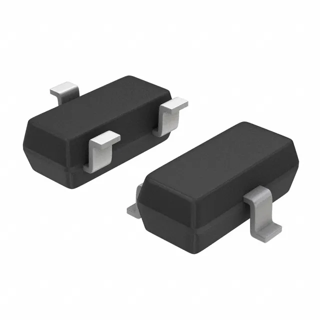
Figure appears in the document as another reliable drop-in alternative. It highlights the features of the onsemi NUP2105L, whose slightly higher reverse stand-off and breakdown voltages (27V / 28V) provide additional design margin against potentially higher voltage transients, suitable for applications with complex power environments or higher robustness requirements.
All three will fit existing PESD2CAN,215 footprints without mechanical change.
If your PCB already integrates a choke before the transceiver, you can mix these variants even across ECUs — their leakage and capacitance differences are small enough that CAN differential symmetry remains stable.
Pro tip: When testing alternates, run a common-mode noise scan up to 500 MHz. If you see new spikes near 250–300 MHz, your Cp is slightly too high for CAN-FD edges.
You can find more examples of component drop-in strategy in TEJTE’s connector replacement guide, which follows the same discipline — verify specs, match mechanicals, and validate performance before mass adoption.
How to lay out pads, vias, and returns to cut clamp overshoot?
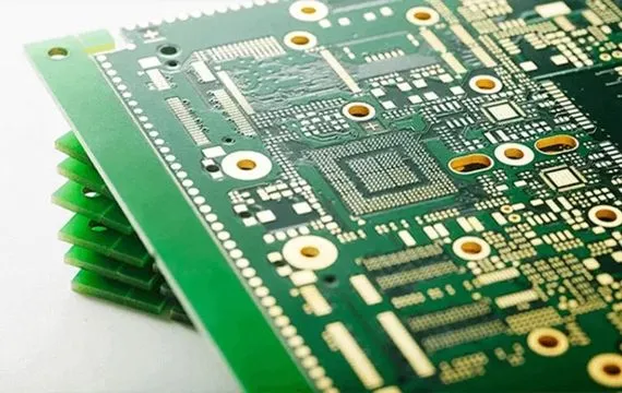
corresponds to the "How to lay out pads, vias, and returns to cut clamp overshoot?" section. It materializes an efficient ESD energy discharge path, emphasizing the decisive role of excellent layout in realizing the performance of TVS diodes.
1. Ground return strategy
When the ESD current hits the CAN connector, it surges through the TVS diode to ground. The faster that current finds a low-impedance return, the lower your overshoot. That’s why layout engineers aim to minimize equivalent series inductance (ESL).
Practical layout tips:
- Place two or more ground vias beside the diode pad; parallel vias halve ESL.
- Keep the ground pour continuous — avoid narrow necks.
- Route CANH/CANL with tight differential spacing right up to the diode.
- If possible, add a small copper island tied to chassis ground near the connector shell to absorb ESD energy before it reaches the logic ground plane.
Measured overshoot tends to follow this empirical rule:
[ V_{overshoot} ≈ di/dt × L_{trace} ]
At 10 A/ns, even 1 nH adds 10 V. That’s why a 5 mm trace at 1 nH/mm can spike 50 V beyond your clamp. Keeping the trace under 3 mm and via-stitching aggressively can reduce the overshoot by 40% or more.
2. Connector spacing guidelines
Field data from automotive ECUs show a practical spacing threshold:
- < 5 mm from connector pin to TVS pad — optimal (typical < 2 V overshoot).
- 5–10 mm — acceptable but risk of > 5 V transient spikes.
- > 10 mm — fails ISO 7637 pulse 3a/3b repeatability in many cases.
3. Example cross-section
CAN/LIN TVS Selection Matrix + Replacement Checklist
TVS Diode Selection Matrix
| Part (M) | Package | VRWM (V) | VBR (min) (V) | VC (max@Ipp) (V) | Ipp (8/20 μs) | Cp (pF @ 1 MHz) | AEC-Q | IEC 61000-4-2 | CAN-FD OK? | Notes |
|---|---|---|---|---|---|---|---|---|---|---|
| Nexperia PESD2CAN,215 | SOT-23 | 24 | ≥ 26.2 | ≤ 41 | 5 A | 25 | ✓ | ±30 kV | – | Classic CAN only |
| ST ESDCAN2-4-2BLY | SOT-23 | 24 | ≥ 26 | ≤ 40 | 5 A | 22 | ✓ | ±30 kV | Partial | Legacy ECU replacement |
| Bourns CDSOT23-T24CAN-Q | SOT-23 | 24 | ≥ 26.2 | ≤ 39 | 5 A | 10 | ✓ | ±30 kV | ✓ | Ideal CAN-FD fit |
| onsemi NUP2105L | SOT-23 | 27 | ≥ 28 | ≤ 41 | 5 A | 17 | ✓ | ±30 kV | Partial | Higher VBR variant |
Rules for quick qualification
- Clamp check:
If VC (max@Ipp) < transceiver ABS MAX and Cp ≤ speed threshold → safe.
- Loss budget:
Overshoot ≈ di/dt × ESL (use 1 nH/mm as quick PCB estimate).
- Replacement filtering:
Match package first, then verify VRWM ≈ 24 V ± 2 V, VBR ≥ 26 V, VC ≤ 41 V.
For CAN-FD, prioritize Cp ≤ 10 pF.
Design tip
- Whenever you integrate ESD diodes in mixed CAN + LIN topologies, check common-mode balance. Even a 3 pF mismatch between lines can distort your bit edge. That’s why modern designs use matched dual diodes with symmetrical routing — exactly the configuration found in PESD2CAN,215 and its drop-in successors.
What mistakes kill ESD compliance most often?
Even seasoned engineers repeat the same few sins when implementing automotive ESD protection — usually because layout, not the diode, betrays them.
- Placing the TVS far from the connector.
Every millimeter adds inductance; every nanohenry adds volts. Keep it right next to the CAN pins.
- Using a power-line TVS on signal lines.
High-capacitance 600 W parts clamp well, but they destroy signal integrity above 1 Mbps. Always use signal-line TVS diodes (SOT-23 or DFN packages) rated for low Cp.
- Ignoring via current sharing.
A single via can saturate; use at least two parallel vias for each diode pad.
- Overlooking adapter or harness stacks.
Each added connector or extension adds reflection points. Test with the final cable assembly attached.
- Skipping post-ESD re-test.
Some failures only appear after multiple 30 kV hits — watch for slow leakage drift or shifted threshold voltages.
Rule of thumb: ESD protection doesn’t just pass once — it passes 1000 times. If you only survive the first pulse, you haven’t protected, you’ve delayed failure.
For a deeper exploration of connector grounding and overshoot reduction, you can revisit TEJTE’s MIMO antenna article, which demonstrates the same high-frequency current path control that keeps ESD safe in differential systems.
Frequently Asked Questions (FAQ)
1. Is PESD2CAN,215 still safe to design in?
2. Will a 24 V TVS diode work for both 12 V and 24 V CAN systems?
3. What capacitance is safe for CAN-FD 5–10 Mbps operation?
4. Can I rely on the transceiver’s internal ESD protection instead?
5. How close should the TVS diode sit to the CAN connector?
6. What are reliable drop-in alternatives to PESD2CAN,215?
Three proven choices stand out:
- ST ESDCAN24-2BLY – same 24 V spec, compatible footprint.
- Bourns CDSOT23-T24CAN-Q – low Cp (~10 pF), CAN-FD ready.
- onsemi NUP2105L – slightly higher VBR (~28 V), robust for harsh nodes.
All are AEC-Q101 qualified and tested under ±30 kV contact discharge.
7. What’s new in 2024–2025 for automotive CAN ESD protection?
Conclusion
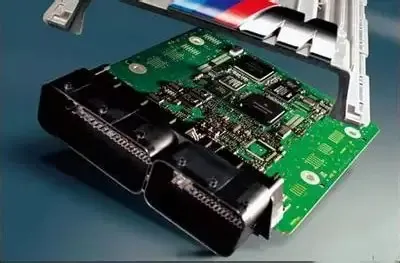
through careful component selection (including alternatives) and rigorous layout practices, robust and compliant CAN bus ESD protection can be achieved, ensuring long-term system reliability.
The PESD2CAN,215 may be entering retirement, but its legacy endures: a clean, reliable, automotive-qualified TVS diode for CAN bus ESD protection that defined the 24 V, 25 pF standard for over a decade.
For classic CAN, it remains perfectly valid — provided you can still source it. For new CAN-FD or mixed 48 V networks, move toward lower-capacitance successors from Bourns, TI, or STMicroelectronics.
In every case, the rules don’t change:
- Choose by spec alignment, not by name.
- Place it as close to the connector as physics allows.
- Verify clamp below ±58 V, and keep Cp under 10 pF for fast buses.
Done right, your CAN transceivers will pass IEC 61000-4-2 testing the first time — and stay quiet for years in the field.
Bonfon Office Building, Longgang District, Shenzhen City, Guangdong Province, China

A China-based OEM/ODM RF communications supplier
Table of Contents
Owning your OEM/ODM/Private Label for Electronic Devices andComponents is now easier than ever.
