Surge Protection Design for 24-V I/O Ports: MOV, TVS & Layout Guide
Dec 14,2025

Placed at the beginning of the article, this image aims to dispel the misconception that risk comes only from the power rail. It visually demonstrates the multiple creative paths surge energy can take to invade 24V control lines—through power lines, long harnesses, relay coil kickback, and near-line coupling—setting the stage for the subsequent discussion on protection solutions.
Which surge scenarios actually hit a 24-V I/O port?
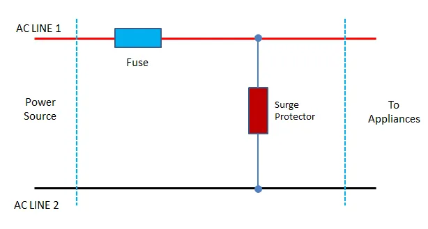
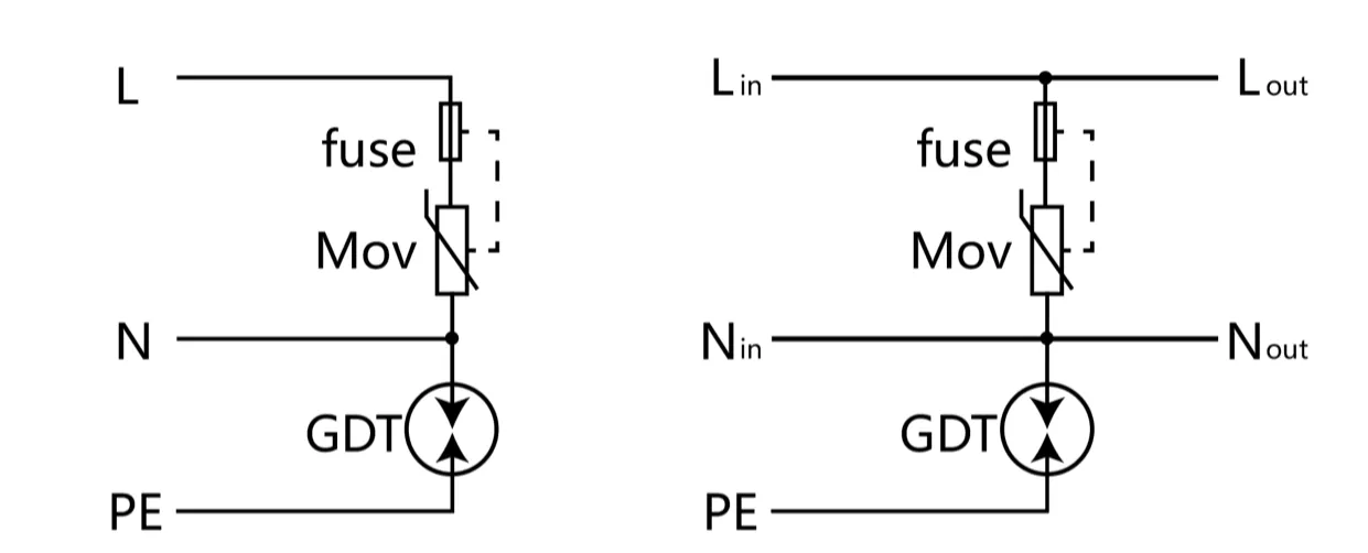
This schematic diagram introduces the basic concept of surge protection. It presents a simplified AC power supply protection scheme, helping readers understand the fundamental principle of primary protection at the power entry point, paving the way for the discussion on more complex multi-stage protection for 24V I/O ports later.
Power line, long harness, relay kick, and near-line coupling
Let’s break down the real-world surge sources that strike 24-V control lines:
- Power-line transients:
Sudden grid switching or industrial machinery startup can inject high-energy pulses through the 24-V supply rail. Even if you’ve got a regulated SMPS, the surge often rides past the input filter before the protection circuit reacts.
- Long cable harnesses:
A 10-m unshielded cable easily builds differential surge voltage due to its inductive impedance. When connected to outdoor sensors or valves, that harness can pick up several hundred volts per microsecond (V/µs) during nearby lightning or motor commutation.
- Relay coil kickback:
A de-energizing relay creates a steep inductive spike that flows through return lines. If multiple relays share a ground trace, a single release can spike the neighboring 24-V I/O channels.
- Near-line or cross-coupling:
In dense control cabinets, surge energy jumps between adjacent cables via capacitance. This is why even isolated analog inputs can fail IEC tests if cabling is bundled too tightly.
Experienced integrators know these hits rarely resemble textbook “clean” pulses. You might see oscillations, mixed polarities, and coupling between multiple nets. The goal isn’t to block them all — it’s to shape them safely into the ground before they hurt your ICs.
Tip from the field: During surge testing, leave at least one “victim” channel open-circuit and one terminated — it reveals if coupling or return routing is your weakest link.
Bridging IEC 61000-4-5 waveforms to field reality
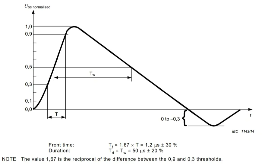
Located in the section discussing “Bridging IEC waveforms to field reality,” this graph highlights the difference between lab-standard test waveforms (e.g., 8/20µs) and the slower, higher-energy, or faster pulses that may be encountered in real installations. It reminds engineers that protection design must consider harsher field conditions, not just passing standard tests.
The IEC 61000-4-5 standard defines 1.2/50 µs open-circuit voltage and 8/20 µs short-circuit current waveforms. Yet real installations often experience mixed forms: slower, higher-energy 10/700 µs surges on long lines, or fast 1 µs spikes from switching MOSFETs.
To interpret lab results correctly:
- Don’t equate “pass” with safety. A test may pass at ±1 kV but fail the first time you connect a 30-m field cable with floating ground.
- Correlate energy, not just voltage. Field pulses tend to carry more joules than their lab counterparts.
- Use 8/20 µs current shape as a baseline for component rating — MOVs, TVS, and GDTs all specify clamping energy in that format.
A practical way to align your design is to test beyond the declared rating. For example, if the compliance level is 1 kV, design your MOV/TVS pair to survive 1.5 kV at least once. The cost difference is trivial, but the robustness gain is dramatic.
(Internal link — dual SOT-23 TVS on 24-V I/O — provides an example of how compact TVS arrays perform under 8/20 µs surges.)
How do you choose and stack MOV vs. TVS effectively?
“Energy vs. clamp” two-axis role map
| Parameter | MOV | TVS Diode |
|---|---|---|
| Response speed | ~25 ns | < 1 ns |
| Energy capacity | High (tens of joules) | Low-medium (mJ range) |
| Leakage current | μA-mA (aging over time) | nA-μA (stable) |
| Voltage tolerance | Wide | Tight |
| Failure mode | Degradation or short | Short/open (depending on polarity) |
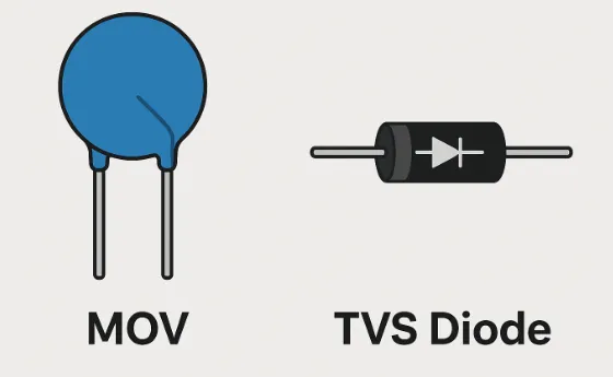
Located after the comparison table in the “How do you choose and stack MOV vs. TVS effectively?” section, this image translates the abstract parameter comparison (e.g., energy capacity, response speed) from the preceding table into an intuitive visual contrast of physical forms using real component photos. Engineers can clearly see that the MOV, responsible for high-energy absorption, is typically larger, while the TVS, tasked with fast and precise clamping, is more compact. This photo reinforces the design philosophy of “energy vs. clamp” division of labor and assists readers in identifying these two critical components during actual PCB layout and part selection.
- MOVs handle the energy dump. They absorb large surge energy (e.g., 1 kA × 8/20 µs) and sacrifice themselves slowly over cycles.
- TVS diodes handle precision clamping. They respond nearly instantly and limit the overshoot within microseconds.
When stacked correctly, the MOV soaks up the high-energy tail while the TVS cleans up the fast edge — a strategy that’s especially critical in PLCs, industrial sensors, and distributed control systems.
To design coordination, plot both clamping curves on the same voltage axis. Ensure that V_MOV residual ≥ V_C of TVS + Δ, where Δ is your routing and common-mode drop margin. This keeps them from “fighting” each other during the event.
(For practical stacking, refer to the TVS diode for surge clamping used in many 24-V designs.)
Coordinated protection: MOV + TVS + GDT
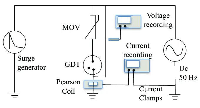
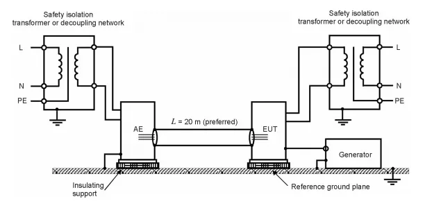
This image appears in the section discussing “Coordinated protection: MOV + TVS + GDT.” It presents a professional test configuration used to verify and coordinate the performance of a multi-stage protection network (GDT, MOV, TVS). The likely inclusion of a current measurement device (Pearson coil) emphasizes the importance of device selection and coordination based on measured data, not just datasheet values.
In more demanding installations — outdoor cabinets or long field runs — you’ll often add a GDT (gas discharge tube) ahead of the MOV. The triple combination behaves like this:
- GDT fires around 230–350 V, handling kiloamp-level events without aging.
- MOV takes the remaining energy after the GDT arc extinguishes.
- TVS clamps the final tens of volts to protect logic inputs and transceivers.
This three-stage network creates a “cascade” of surge handling — each stage progressively tighter and faster.
Example configuration:
Field line ─┬── GDT ─── MOV ─── TVS ──► Protected I/O
│
└─→ Earth return (short path)
Design tip: Always place the GDT and MOV close to the connector, with direct paths to chassis ground. The TVS should sit at the PCB entry point of your circuit domain, near the IC pins.
Unlike purely theoretical circuits, this hybrid topology survives both high-energy lightning pulses and smaller switching surges. You’ll find it in PLC I/O boards, machine tool controllers, and distributed sensor hubs.
For detailed insight into ESD-level behavior of TVS diodes in high-speed lines, see TEJTE’s low-cap TVS for HDMI/USB — it complements surge-grade design with fine-tuned signal protection.
Field note
How to align clamp voltage to Abs Max without false conduction
Working limits for V_WM / V_BR / V_C with tolerances
Every TVS diode datasheet lists three critical parameters:
- V_WM (Working Peak Voltage): the continuous voltage where the diode stays non-conductive.
- V_BR (Breakdown Voltage): the point where conduction starts (typically defined at 1 mA).
- V_C (Clamping Voltage): the voltage measured during a defined surge pulse (e.g., 8/20 µs at a specific current).
The right way to pick a part isn’t to find “one number between 24 and 40.” Instead, you calculate margins across both normal and surge conditions.
To stay safe:
- (V_{WM} \ge 0.9 \times V_{max}) ensures your 24-V rail doesn’t bias the TVS too close to leakage.
- (V_C(max) \le 0.95 \times V_{absmax}) prevents clamping from overshooting your IC’s rating.
For example:
If your 24-V port runs up to 28.8 V, and the IC can tolerate 40 V max, you’ll need a TVS with
(V_{WM} ≥ 26 V) and (V_C(max) ≤ 38 V.)
Note: Some engineers try to lower V_C aggressively for “tighter” protection, but that usually increases leakage or even steady-state conduction. Once the diode leaks, EMC and power loss issues appear — ironically defeating the purpose of surge protection.
Two do-not-break rules: avoid normal-mode leakage and over-clamp
There are two simple yet often-ignored ground rules when aligning clamp voltage:
- Avoid normal-mode conduction.
If your TVS conducts even slightly during normal 24-V operation, it will heat and age rapidly. Within months, it’ll drift down in V_BR and start clamping prematurely. That’s why the 0.9 × V_max rule exists — it’s your safety cushion.
- Avoid over-clamp crossing.
When V_C(max) exceeds the downstream device’s Abs Max, the TVS stops being a protector and becomes the failure trigger. A spike that should have been absorbed instead punches through the IC’s ESD diodes.
In real-world debugging, you’ll recognize this instantly: the port survives low-level hits but dies during the first high-energy surge. Always re-check V_C(max) against your component’s worst-case Abs Max, including temperature drift.
This is exactly why TEJTE developed its internal Clamp-Fit Calculator, which automates the voltage coordination between MOV, TVS, and system Abs Max.
24-V Clamp-Fit Calculator

Serving as an illustration for the “24-V Clamp-Fit Calculator” section, this image likely depicts an integrated protection module product from TEJTE. Using a concrete product example, it materializes the theoretical concepts of voltage coordination and multi-stage protection discussed earlier, providing engineers with a reference for a potential ready-to-use solution.
| Input Field | Example Value | Purpose |
|---|---|---|
| Nominal Port Voltage (Vnom) | 24.0 V | Normal operation voltage |
| Maximum Port Voltage (Vmax) | 28.8 V | Worst-case regulated voltage |
| Protected Device Abs Max (Vabsmax) | 40.0 V | From IC datasheet |
| TVS Working Voltage (VWM) | 26.0 V | TVS nominal threshold |
| TVS Breakdown Voltage (VBR min) | 28.9 V | Start of conduction |
| TVS Clamping Voltage (VC max, 8/20 μs) | 37.5 V | Surge clamping limit |
| MOV Residual Voltage (VMOV residual, 8/20 μs) | 45.0 V | From MOV datasheet |
| Routing / Common-mode Drop | 1.5 V | PCB + choke + ground drop |
Computation Logic
1. Check working margin: V_WM ≥ 0.9 × V_max
2. Check safe clamping: V_C(max) ≤ 0.95 × V_absmax
3. Check stage coordination: V_MOV_residual ≥ V_C(max) + Δ
Output Example
| Check | Result | Comment |
|---|---|---|
| Working Margin | Pass | TVS remains off during 24-V operation |
| Safe Clamping | Pass | 37.5 V ≤ 38.0 V (OK) |
| Stage Coordination | Pass | 45.0 ≥ 39.0 (OK) |
Recommendation:
If any check fails, either increase V_WM slightly (to reduce leakage) or pick a lower V_C(max) model. For MOV misalignment, select a higher voltage rating to avoid premature conduction overlap.
(Reference: for circuit damping before the protection chain, see relay/motor damping vs surge — it explains how snubbers complement surge absorbers.)
Where should TVS/MOV/GDT sit on the PCB and why?
Connector-side first, shortest loop, nearest ground
The first golden rule: protection belongs at the connector, not beside your MCU.
- TVS placement: always right at the interface pin — the first component hit by surge energy.
- Return path: minimize loop area. The return to chassis or ground should travel straight, not through narrow traces or vias.
- Grounding: use a low-impedance chassis reference or polygon pour. Don’t share digital grounds for surge return.
A practical way to visualize current flow is to draw a “surge loop” in CAD. If the loop exceeds 2–3 cm, you’re adding inductance that can spike another 10–15 V during fast transients.
(For advanced RF-style grounding methods under surge conditions, TEJTE’s port grounding under transients provides an interesting parallel.)
Ordering with CM chokes, terminations, and RC snubbers
In mixed-signal or sensor boards, the protection chain often overlaps with EMI filters and line terminations. The general sequencing rule goes like this:
Connector → GDT → MOV → CM Choke → TVS → RC Snubber → IC
- Common-mode chokes (CMCs) should sit after surge arresters, not before — otherwise, the surge energy saturates the choke before it can attenuate noise.
- RC snubbers are for energy damping within the IC’s range; they complement the TVS by controlling ringing and secondary overshoot.
- Terminations (resistors, optocouplers, or transceivers) must connect after the TVS to stay safe from direct current injection.
When routing these components, always:
- Keep the GDT and MOV pair as close to the connector ground as possible.
- Route the TVS branch with minimal via count.
- Avoid stitching vias under the CMC — they often increase coupling.
Field placement example
Located in the “Field placement example” subsection, this is a key visual connecting theory to practice. Based on a TEJTE reference design, it intuitively demonstrates how to place protection devices like GDT and MOV close to the connector and plan low-impedance return paths. The annotated dimensions (e.g., 1.5mm via spacing) and layout results (clamping MCU pin voltage from 45V to 33V) provide engineers with quantifiable layout guidance.
On a TEJTE reference I/O board:
- A 350-V GDT and 14-mm MOV sit right at the terminal block input.
- The bidirectional SOT-23 TVS (TEJTE P/N TJT23B-33CA) sits 5 mm away from the MCU I/O connector.
- Ground via spacing: 1.5 mm, with direct stitching to chassis pour.
- All return loops are under 10 mm effective length.
This simple placement cut the surge rise at the MCU pin from 45 V to 33 V during ±1 kV, 8/20 µs hits.
How do you turn IEC 61000-4-5 into a practical port test matrix?
Level × Port × Injection Matrix
This image is in the chapter “How to turn IEC 61000-4-5 into a practical port test matrix.” It visualizes and concretizes the abstract test standard, providing a matrix template categorized by port type, test level, injection method, and protection path planning. This graph is a powerful tool for systematic pre-compliance design and failure prediction, guiding engineers to move beyond a checkbox mentality and proactively plan protection strategies.
| IEC 61000-4-5 Level | Voltage (Line-to-Ground) | Port Type | Injection Method | Suggested Surge Path |
|---|---|---|---|---|
| Level 1 | ±500 V | Logic I/O, sensors | Coupling clamp | MOV + TVS only |
| Level 2 | ±1 kV | Short field cables (<10 m) | Direct contact | GDT + MOV + TVS |
| Level 3 | ±2 kV | Long cables, outdoor I/O | Direct contact | GDT + MOV + TVS + choke |
| Level 4 | ±4 kV | Power & communication hybrids | Differential injection | MOV + RC damping + shielding |
| Custom / Field | 1-6 kV mixed | 24-V distributed I/O | Real-cable test | Verify grounding loops |
How to use it:
- Start with the highest level you expect, not the lowest your customer requires.
- For mixed I/O (analog + digital), apply the worst case across all lines.
- Add “fail mode” notes — such as “relay chatter,” “ADC offset,” or “MCU reset.” They reveal where your protection is weak.
Cable length and grounding choices
In real installations, cable length multiplies surge risk.
Every additional meter of unshielded cable adds roughly 1–2 µH of inductance — translating to 2–5 V/µs extra overshoot per ampere of surge current.
Grounding is equally critical:
- Star grounding minimizes common-mode rise between I/O groups.
- Chassis bonding at the entry point prevents GDT arcs from jumping across signal planes.
- Floating grounds may pass ESD tests but fail surge; always include a defined return conductor.
Pro tip: During pre-compliance, use a low-cost surge generator with adjustable pulse width to fine-tune your cable layout before renting a certified lab. You’ll save both time and prototypes.
Can we close with a one-page “energy–cost–BOM” decision table?
24-V I/O Surge-Protection BOM Decision Table

This image is part of or a visual summary for the “24-V I/O Surge-Protection BOM Decision Table.” Through a concise chart, it highlights the complementary roles of the three main types of protection devices: TVS (fast, precise clamping), MOV (medium energy absorption), and GDT (high energy discharge but slower). This comparison is fundamental to designing multi-stage coordinated protection schemes.
| Tier | Use Case | Typical Surge Level | Component Stack | Approx. Cost Impact | Comments |
|---|---|---|---|---|---|
| Entry (Basic) | Indoor PLC modules, short cables | ±1 kV (8/20 μs) | Bidirectional TVS only | +2 % | Small SOT-23 works if surge energy < 20 A |
| Mainstream (Balanced) | Factory I/O, relay control | ±2 kV (8/20 μs) | MOV + TVS | +5 % | Best price-to-robustness ratio; fits most 24-V systems |
| High-Robust (Field) | Outdoor or distributed I/O | ±4 kV (10/700 μs) | GDT + MOV + TVS + RC snubber | +8 – 10 % | Survives multiple surge cycles; suitable for IP67 equipment |
Each tier uses the same footprint for interchangeability. When a project moves from Entry to High-Robust, your PCB can stay identical — you simply populate more components.
(If you’re designing from scratch, start with the Industrial surge protection guide hub to cross-reference related compliance topics.)
Common traps (ESD plan ≠ surge plan, etc.)
- Mistaking ESD parts for surge parts:
A 5 V ESD TVS may handle ±15 kV air discharge but only a few amps of 8/20 µs current. That’s orders of magnitude below a real surge.
- Ignoring cumulative stress:
MOVs degrade every hit; test boards after 100 pulses, not just one.
- Over-filtering:
Excessive RC or LC filters slow the rise time but also distort analog signals or CAN edges.
- Neglecting thermal protection:
For panel SPDs, always pair MOVs with thermal fuses or self-disconnect links — required by UL 1449:2025.
What’s new in 2025 without repeating news all over the article?
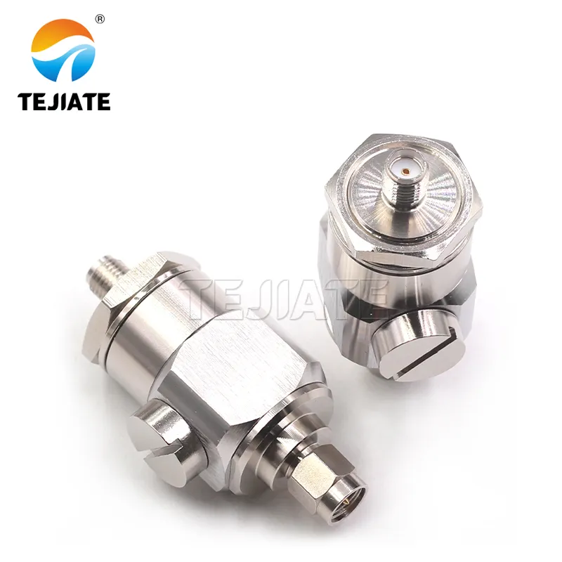
Serving as the illustration for the “What’s new in 2025?” section, this image moves away from an abstract infographic to directly present a physical product from TEJTE that corresponds to the new developments. It visually bridges the temporal concept of “2025 updates” with a concrete, procurable component, giving engineers a direct visual reference. The photo likely highlights the new product’s packaging improvements, increased power density, or features compliant with new standards (e.g., UL 1449:2025), thereby grounding industry trends in specific component choices.
Staying current matters — but repetition kills readability. Here’s a quick snapshot of the 2025 updates worth noting once:
- UL 1449 (Oct 2025 Revision) — Adds Type 5 SPD category, clarifies short-circuit current tests, and introduces sustained-voltage endurance requirements for DC power sources. Expect panel-level SPD datasheets to list new “MCOV-DC” ratings.
- Bourns 1202-P Series (Type 1 SPD, Dec 2025) — Thermally protected MOV stack rated 40 kA (8/20 µs), ideal for service-entrance panels.
- Littelfuse 3 kA Compact TVS (Sept 2025) — Doubles energy density for PoE and DC-bus protection in SMD footprints.
- TDK Hybrid MOV + GDT (Dec 2025) — Combines zero-leakage GDT behavior with MOV energy handling, extending life by 3× in surge endurance tests.
Frequently Asked Questions
1. Should I use MOV, TVS, or both for a 24-V input port?
Use both if space allows. The MOV absorbs high-energy surges; the TVS limits residual voltage to protect ICs.
2. How do I set a clamp voltage that won’t exceed my MCU Abs Max?
Follow the calculator rules: (V_C(max) ≤ 0.95 × V_{absmax}). For a 40 V device, keep clamp ≤ 38 V.
3. Where exactly should the TVS sit — connector side or near the IC?
Always connector-side first. The return path must be short and direct to chassis ground.
4. What IEC 61000-4-5 level makes sense for small PLC I/O vs. field devices?
Level 2 (±1 kV) suits indoor PLCs; Level 3–4 (±2 – 4 kV) for outdoor or distributed I/O.
5. Can an ESD-only design pass surge once the cable run exceeds 3–5 m?
Unlikely. Cable inductance amplifies transients faster than ESD parts can respond. Add a MOV stage.
6. How do I coordinate MOV residual voltage with a downstream TVS without overlap loss?
Ensure (V_{MOV residual} ≥ V_C(max) + Δ) (where Δ ≈ 1–2 V routing drop).
7. What changes with UL 1449’s 2025 revision when selecting panel SPDs?
Expect mandatory thermal disconnects and clearer Type 5 markings for DC applications.
Final Thought
A well-designed 24-V I/O protection network isn’t defined by one magic component. It’s the coordination — energy staging, voltage alignment, and layout discipline — that separates a “passed test” from a system that survives ten years in the field.
Engineers who document their surge matrix, simulate clamp behavior, and validate grounding early rarely face late-stage redesigns. And that’s the quiet reward of good surge design: nothing happens — ever — when it should have exploded.
Bonfon Office Building, Longgang District, Shenzhen City, Guangdong Province, China

A China-based OEM/ODM RF communications supplier
Table of Contents
Owning your OEM/ODM/Private Label for Electronic Devices andComponents is now easier than ever.
