Small Signal MOSFET Selection Guide
Jan 5,2026

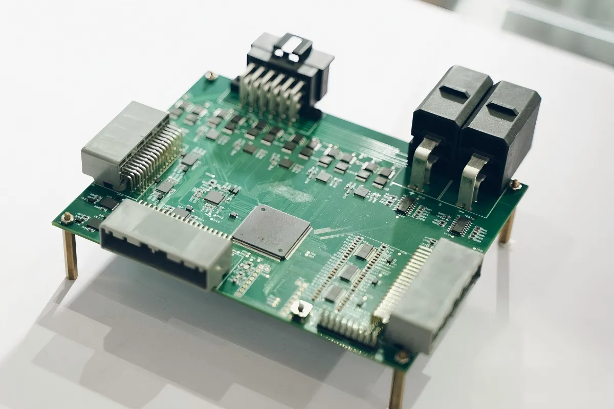
This figure typically shows a typical N-channel enhancement-mode MOSFET structure, helping engineers understand the basic working principle of the device, especially its role in low-voltage, low-current applications.
A small signal MOSFET almost never feels like a design decision worth debating. It is small. It is cheap. It fits anywhere. Most of the time, it is added after the MCU pinout is already fixed and the power tree looks “good enough.”
That is exactly why it causes trouble.
On modern MCU boards, the small signal MOSFET often ends up carrying more responsibility than intended. It gates sensor rails, buffers fragile GPIOs, switches loads under PWM, and quietly absorbs abuse from firmware experiments. When it is poorly chosen, nothing fails outright. Things just feel off—voltage drops that should not be there, parts that run warm for no obvious reason, or logic-level devices that never seem fully on.
This guide is written from that angle. Not theory first. Not datasheet worship. Just the practical way engineers end up learning how to choose small signal MOSFETs for MCU and sensor designs.
Why do small signal MOSFETs matter in modern MCU boards?

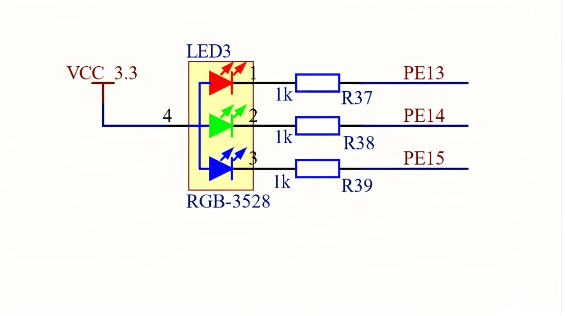
The figure shows a typical MCU board-level design where small signal MOSFETs are used to control an RGB LED. The circuit includes current-limiting resistors and GPIO connections, illustrating the use of MOSFETs in low-side switch configurations.
MCU boards today are constrained in ways older designs were not. GPIO pins source less current. Supply rails are tighter. Peripheral loads are expected to sleep aggressively and wake instantly. All of that pushes stress into places designers used to ignore.
The small signal MOSFET sits right at that boundary.
It is often the first active device between a clean digital pin and an unpredictable load. Once you notice that, it becomes obvious why its behavior matters more than its size suggests.
Understand what “small signal MOSFET” means in practice
There is no checkbox in a datasheet that says small signal. Engineers use the term because it maps to how the device is actually used.
In practice, these MOSFETs share a few traits:
- Drain-source voltages usually below 30 V, sometimes up to 50–60 V
- Load currents that rarely exceed an ampere
- Packages small enough that copper area, not silicon, sets the thermal limit
- Gate drive that comes straight from logic, not a driver IC
If a MOSFET expects a strong gate driver or relies on a heatsink, it no longer belongs in this category. Small signal parts assume the board is doing most of the work.
That assumption is fine—until it isn’t.
See where small signal MOSFETs replace BJTs in real designs
Many designs still start with a BJT, especially when the load current looks modest. The switch to a MOSFET usually happens after something feels inefficient rather than broken.
Common triggers include:
- LED indicators that waste too much voltage headroom
- Sensor rails that sag under load for no clear reason
- GPIO pins running close to their absolute limits
- PWM loads that make a transistor noticeably warm
Once a MOSFET replaces the BJT, designers rarely go back. The improvement is not subtle, especially on 3.3 V systems where every tenth of a volt matters.
Learn how small signal MOSFETs reduce power loss and heat
The math is simple, but the consequences are easy to underestimate.
A BJT dissipates power based on its saturation voltage. That voltage does not scale down just because your system voltage does. At a few hundred milliamps, it adds up faster than most people expect.
A MOSFET, once properly driven, behaves like a resistor. Loss scales with current squared:
- BJT: loss ≈ saturation voltage × current
- MOSFET: loss ≈ current² × Rds(on)
On a dense MCU board, that difference often decides whether thermal concerns stay theoretical or show up in testing.
How should you read a small signal MOSFET datasheet for IO and sensor loads?
Datasheets are exhaustive by design. That does not mean you should read them exhaustively.
For small signal MOSFETs, most parameters only matter after you have already made the right coarse selection. The trick is knowing which numbers to look at first.
Focus on Vdss, Id, Rds(on), and package power limits first
These four parameters eliminate most bad choices quickly.
- Vdss sets your survival margin. A common engineering habit is choosing at least 1.5× the nominal supply voltage to cover spikes and ringing.
- Id is rarely the real limit. Thermal conditions usually cap usable current long before silicon does.
- Rds(on) defines conduction loss. It only matters at the gate voltage you actually apply.
- Package power dissipation tells you whether the part can survive steady operation without turning the PCB into a heatsink.
On small packages, power dissipation—not current rating—is usually the real constraint.
Interpret Vgs(th), logic level specs, and gate charge (Qg)

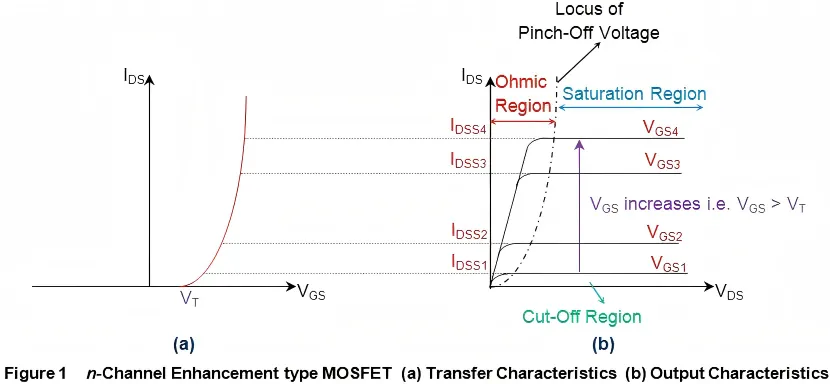
This curve diagram illustrates the relationship between MOSFET threshold voltage (Vgs(th)) and on-resistance (Rds(on)), helping engineers understand the conduction behavior of MOSFETs under logic-level drive.
This is where many selections quietly go wrong.
Threshold voltage does not mean “on.” It means barely conducting. A MOSFET with a low Vgs(th) can still have unusable Rds(on) at 3.3 V.
For MCU-driven designs, you care about:
- Rds(on) specified at your IO voltage
- Whether the part truly behaves as a logic level MOSFET
- Gate charge, especially if you plan to switch often
This distinction becomes obvious in designs that use the device explicitly as a switch, as discussed in MOSFET as a switch design for low-power loads.
Check SOA and dV/dt limits for safe switching
Small signal MOSFETs fail in quiet ways. Spending too much time in the linear region, or repeatedly switching inductive loads without protection, slowly degrades them.
The SOA curve is not just for power devices. It tells you whether a MOSFET tolerates brief overloads or startup stress without aging prematurely.
How do you classify small signal MOSFET options for different applications?
Group small signal MOSFETs by voltage and current ranges
In real projects, most devices fall into a few buckets:
- Voltage ratings around 20 V, 30 V, or 50 V
- Continuous currents below 0.5 A, between 0.5 A and 1 A, or slightly above
MCU boards rarely need more than that. Knowing this early prevents unnecessary over-specification.
Compare N-channel vs P-channel and enhancement vs depletion
For switching, the n channel MOSFET transistor is usually the obvious choice. Lower resistance and better availability make it hard to justify alternatives.
P-channel devices still appear in high-side roles, but designers typically accept their higher losses in exchange for simpler control.
Depletion-mode parts are uncommon and usually avoided unless a very specific behavior is required.
Map package types to board constraints
Package choice affects more than footprint.
Smaller packages reduce space but leave little thermal margin. Slightly larger packages often lower temperature rise dramatically with minimal area penalty. DFN packages spread heat well but demand tighter assembly control.
On compact sensor boards, this trade-off often matters more than headline electrical ratings.
How can you select a small signal MOSFET step by step for your design?
Most selection mistakes happen before anyone opens a datasheet. The error is not technical—it is procedural. Engineers jump straight to part numbers without first fixing the electrical boundaries of the problem.
A reliable selection flow feels slower at first. In practice, it saves time because it eliminates backtracking later.
Define load voltage, current, and switching frequency
Start with the load, not the MOSFET.
Write these numbers down, even if they feel obvious:
- Supply voltage seen by the load
- Maximum steady-state current (not average)
- Whether the load is static, switched occasionally, or PWM-driven
This step sounds trivial, yet many designs skip it. That is how a MOSFET ends up operating at the edge of its thermal envelope without anyone noticing.
For example, a sensor rail that draws only 80 mA on average may briefly pull 200 mA at startup. That transient often defines the real stress point.
Derive minimum Vdss, Rds(on), and package power ratings
Once the load is defined, the MOSFET requirements fall out naturally. This is where a simple calculation-based table helps more than intuition.
Below is a Small Signal MOSFET Selector Table designed for quick screening rather than final approval.
Small Signal MOSFET Selector Table
| Application type | Vsupply V | I_load_max_A | Fswitch kHz | Vdroptarget V | Rds_on_max_required_Ω | Pdiss W | Vdss_min_required_V | Package Pdiss_limit W | Thermal margin score | Logic_level_required_flag |
|---|---|---|---|---|---|---|---|---|---|---|
| LED indicator | 3.3 | 0.02 | 0 | 0.05 | 2.5 | 0.001 | 5 | 0.25 | 250 | YES |
| Sensor rail | 3.3 | 0.15 | 0 | 0.05 | 0.33 | 0.007 | 5 | 0.30 | 43 | YES |
| Small relay | 5 | 0.12 | 0 | 0.10 | 0.83 | 0.012 | 8 | 0.35 | 29 | MAYBE |
| Tiny fan | 12 | 0.30 | 20 | 0.20 | 0.67 | 0.060 | 18 | 0.50 | 8.3 | MAYBE |
Key formulas used
• Rds_on_max_required = Vdrop_target_V / I_load_max_A
• P_diss_W = I_load_max_A² × Rds_on_max_required
• Vdss_min_required = 1.5 × V_supply_V
• Thermal_margin_score = Package_Pdiss_limit_W / P_diss_W
Thermal margin interpretation
- ≥ 3 → High margin
- 1.5–3 → Medium margin
- < 1.5 → Low margin, change device or package
This table does not pick the MOSFET for you. It tells you whether your assumptions are sane. If the thermal margin score is already low on paper, no layout trick will save it later.
Filter candidates by gate drive voltage and logic-level behavior
Only after electrical and thermal limits are clear does gate drive become the focus.
This is where many “logic level” parts quietly disappoint. A MOSFET can meet every current and voltage requirement and still perform poorly if its Rds(on) is specified only at 4.5 V while your MCU outputs 3.3 V—or worse, 1.8 V.
At this stage:
- Discard parts without Rds(on) data at your gate voltage
- Be skeptical of parts where the only low-voltage spec is Vgs(th)
- Pay attention to Qg if switching frequency is nontrivial
Designers who routinely work with mixed-voltage systems often formalize this check using approaches similar to those described in logic level shifter design for I2C and mixed-voltage MCUs.
Rank devices by cost, availability, and supplier risk
Only now does cost matter.
In low-power designs, the price difference between two suitable MOSFETs is usually negligible compared to the cost of redesign or field issues. Long-term availability, second sources, and consistent parametric behavior often outweigh a few cents of savings.
Many experienced teams deliberately avoid the “best” MOSFET on paper and choose the one with comfortable margin and stable supply.
How do you design MCU IO and GPIO stages using small signal MOSFETs?

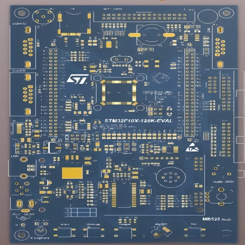
The figure shows an actual PCB layout emphasizing the placement of small signal MOSFETs close to loads (such as connectors or sensors) to optimize current paths, reduce parasitic resistance and loop area, and improve overall performance and thermal management.
Thermal problems with small signal MOSFETs are rarely caused by the silicon itself. They are almost always layout problems that only become visible once the board is assembled.
Because these devices are small, designers tend to treat them like logic ICs. That assumption breaks down the moment the MOSFET carries real current.
Place critical small signal MOSFETs near their loads
Distance matters more than many people expect.
Placing a MOSFET close to its load reduces:
- Trace resistance that quietly adds voltage drop
- Loop area that invites EMI during switching
- Ground bounce that can couple back into MCU pins
On dense MCU boards, moving a MOSFET a few millimeters closer to a connector or sensor often improves behavior more than changing the part number.
Use copper area and vias to manage power dissipation
Small packages shed heat through copper, not air.
For SOT-23 or SOT-523 devices:
- A modest copper pour on the drain can dramatically lower thermal resistance
- Thermal vias help only if they connect to real copper on inner or bottom layers
- Solder mask openings can matter when margins are tight
Designers sometimes assume that “low current” means “no thermal design needed.” In practice, even tens of milliwatts can push junction temperature uncomfortably high in cramped layouts.
Avoid gate noise coupling and unintended switching
Gate pins are sensitive. Treat them that way.
Common mistakes include routing the gate trace parallel to fast-switching power paths or leaving it long and unterminated. When unexplained switching or heating appears, adding a small gate resistor or RC filter often reveals that the problem was noise, not logic.
What protection and reliability practices keep small signal MOSFETs alive?
Combine MOSFETs with flyback and clamping components
Any inductive load deserves respect, no matter how small it looks.
Relays, motors, and even long cables can generate voltage spikes that exceed Vdss in an instant. A flyback diode, TVS, or clamping network is usually cheaper than replacing a board.
Designers who want a deeper look at protection patterns often reference discussions similar to those in flyback and TVS protection for MOSFET-switched loads.
Respect avalanche, ESD, and latch-up limits in sensor interfaces
Sensor interfaces are exposed by nature. Cables get plugged in hot. Grounds shift. ESD events happen when no one is watching.
Even if a MOSFET survives a single event, repeated stress can degrade it quietly. Respecting avalanche energy limits and adding upstream protection improves long-term reliability far more than oversizing the MOSFET alone.
Plan for automotive or industrial-grade devices when needed
Not all environments are equal.
In automotive or industrial systems, temperature swings, vibration, and electrical noise push small signal MOSFETs beyond consumer assumptions. In these cases, choosing qualified parts is less about headline specs and more about consistency over time.
What are the latest trends in the small signal MOSFET market?
Follow growth of the global MOSFET and small signal segments
Industry forecasts consistently show steady growth for MOSFETs overall, with small signal devices tracking closely behind. This growth is not driven by high power applications, but by sheer volume in low-power electronics.
For designers, the implication is simple: availability is generally good, but popular parts can still disappear when demand spikes.
Note how IoT and sensor modules drive small signal discrete demand
IoT nodes, sensor hubs, and edge devices use small signal MOSFETs everywhere—often several per board.
As these products multiply, manufacturers optimize for:
- Lower gate charge at logic-level voltages
- Predictable Rds(on) at 1.8 V and 3.3 V
- Smaller packages that still tolerate modest power
This trend reinforces the importance of understanding real operating conditions rather than relying on generic “logic-level” labels.
Watch newer low-voltage and trench-based MOSFET families
Process improvements continue to lower Rds(on) without increasing die size. Trench-based devices in particular have improved switching speed and thermal behavior at low voltages.
For engineers, the practical takeaway is incremental, not revolutionary: newer families often buy a bit more margin, not a license to ignore fundamentals.
How do you debug common small signal MOSFET issues in real projects?
Why does a small signal MOSFET run hot at low currents?
When a MOSFET runs hot “despite low current,” the cause is usually one of three things:
- Rds(on) is much higher at the actual gate voltage than expected
- The device is spending time in the linear region due to slow or noisy gate drive
- Thermal dissipation is limited by layout, not silicon
Measuring gate voltage under load often reveals the issue faster than thermal probing.
Why does my logic-level MOSFET not turn fully on at 1.8 V or 3.3 V?
This is almost always a datasheet interpretation problem.
Vgs(th) misleads many designers into assuming functionality at low voltage. In reality, only Rds(on) curves at the actual gate voltage tell the truth. This failure mode appears repeatedly in community discussions and practical guides.
How can you quickly sanity-check a small signal MOSFET choice on the bench?
A simple approach works well:
- Apply the maximum expected load
- Let the board reach thermal steady state
- Measure voltage drop and temperature rise
Comparing these measurements with the calculated dissipation and thermal margin from the selection stage often confirms—or disproves—your assumptions.
When should you upgrade from a small signal MOSFET to a power MOSFET or driver IC?
Upgrading is justified when:
- Thermal margin consistently falls below comfortable levels
- Switching speed requirements increase
- Gate drive becomes marginal or noisy
At that point, complexity buys reliability.
Bonfon Office Building, Longgang District, Shenzhen City, Guangdong Province, China

A China-based OEM/ODM RF communications supplier
Table of Contents
Owning your OEM/ODM/Private Label for Electronic Devices andComponents is now easier than ever.
