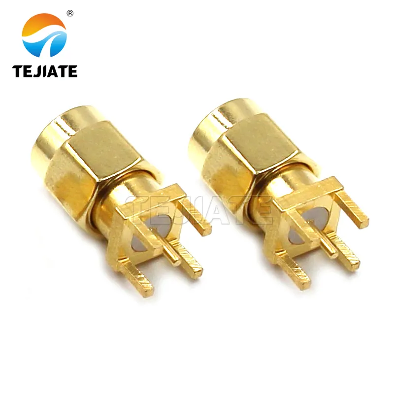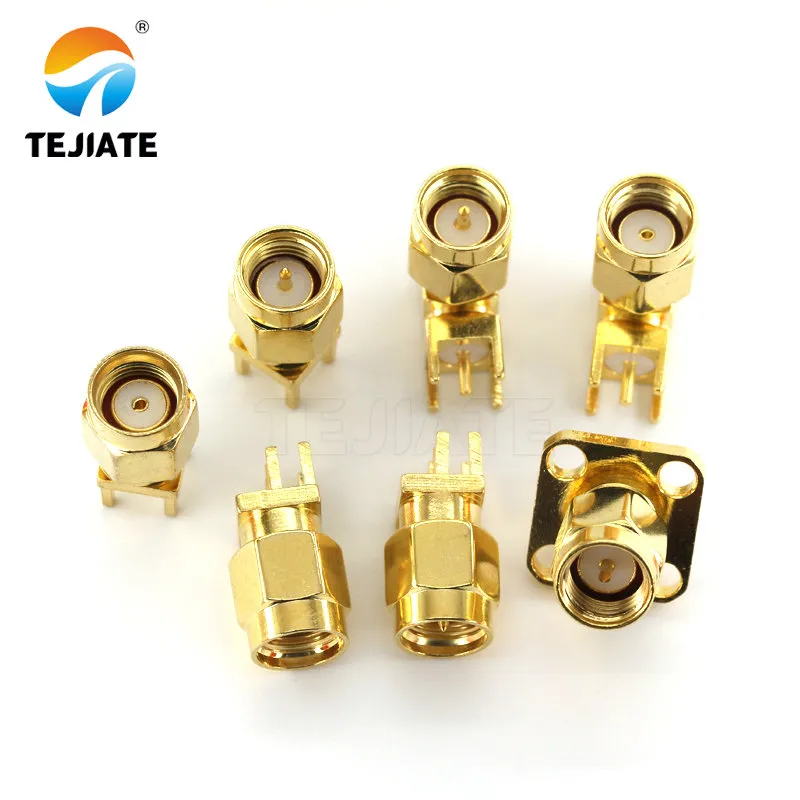
SMA Connector PCB Layout: Tips for 50Ω Launch & Routing
Designing an RF board is always a balancing act. On the CAD screen, the traces look neat and predictable, but in practice the way you implement an sma connector pcb layout often determines whether the design performs flawlessly above 2 GHz or ends up failing during lab validation. A pad that’s slightly oversized, a ground clearance that’s too tight, or a missing via fence can shift impedance by just a few ohms. That small change is enough to cause reflections, bandwidth reduction, and, in the worst case, another costly board spin.