MOSFET as a Switch: Small-Signal Design Guide
Jan 4,2026
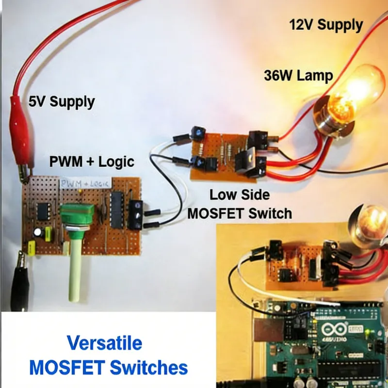
Located below the article title, this is a conceptual schematic. It builds the foundational scenario for the entire discussion using the most simplified elements (power supply, logic signal, MOSFET, load), visually conveying the message that “MOSFET switches are ubiquitous and critical,” laying the groundwork for subsequent in-depth analysis of parameters, selection, and failure modes.
Using a MOSFET as a switch often feels like the most straightforward decision in a low-power design. One GPIO pin, one transistor, one load. Simple enough.
Yet in real products, that single decision quietly determines efficiency, thermal margin, EMI behavior, and long-term reliability.
In MCU-based systems—sensor nodes, control boards, small actuators—the small signal MOSFET switch is everywhere. Ironically, it’s also one of the least scrutinized parts of the schematic. Engineers tend to assume that “any MOSFET will work,” especially when currents look modest on paper.
This guide is written for engineers who have already been burned once—or want to avoid that experience entirely. Instead of repeating definitions, we’ll focus on how MOSFET switches behave in real boards, how to read datasheets without falling into common traps, and how to size margin that survives temperature, tolerance, and abuse.
Why use a MOSFET as a switch for low-power loads?
Compare MOSFET and BJT behavior in pure switching roles
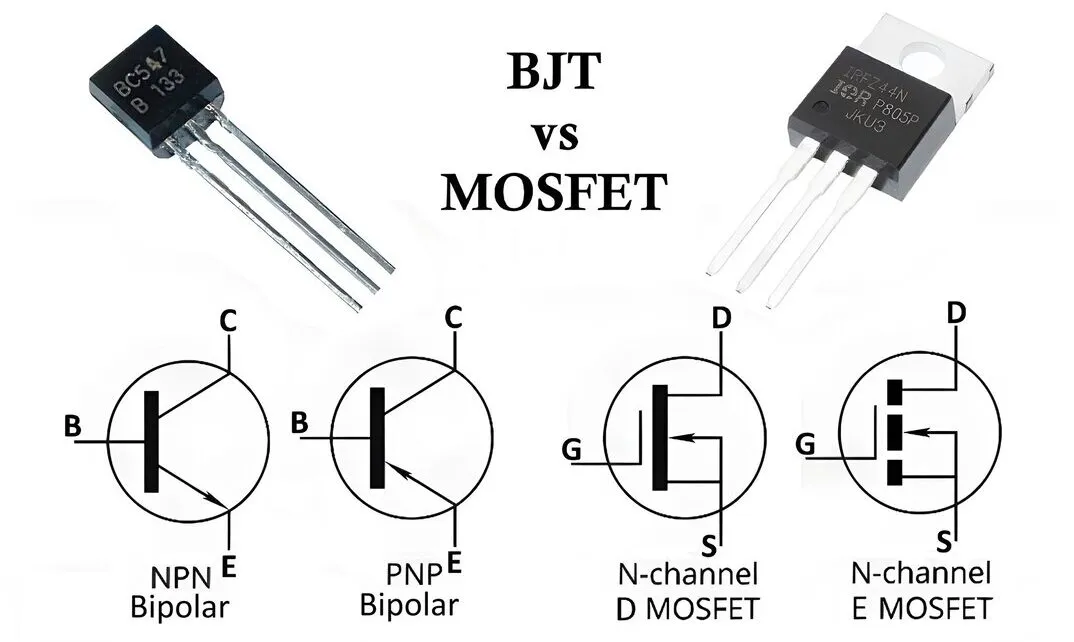
This figure is the core illustration of the technical comparison section. Its purpose is not to show a specific circuit but to emphasize the difference in working principles through symbol comparison. This difference directly determines why MOSFETs are often the better choice in low-power MCU designs, steering the discussion from “what” to “why.”
Both BJTs and MOSFETs can be used as switches. On a schematic, the difference looks cosmetic. Electrically, it is not.
A BJT used as a switch operates in saturation. Once saturated, the collector–emitter voltage drop is relatively fixed—typically a few hundred millivolts. That means conduction loss scales linearly with current. At 20–30 mA, this is rarely a concern. At several hundred milliamps, it becomes a thermal issue surprisingly fast.
A MOSFET as a switch, when fully enhanced, behaves more like a resistor than a voltage drop. Conduction loss follows I² × Rds(on). That quadratic relationship sounds worse on paper, but in practice the Rds(on) can be so low that total loss is dramatically smaller than a saturated BJT.
Drive behavior matters just as much. A BJT requires continuous base current to remain saturated. That base current comes from the MCU pin, a resistor network, or another transistor stage. A MOSFET, by contrast, draws current only during gate charge and discharge. Once the gate is charged, steady-state current is essentially zero.
In low-power MCU designs, that difference often decides whether a GPIO pin is comfortably within spec—or quietly overstressed.
Identify where MOSFET switches shine in MCU-based designs
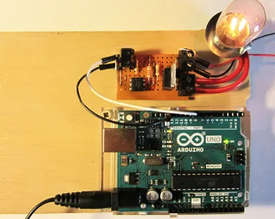
This figure connects theory with practice, providing specific design context. It helps readers map the abstract concept of a “MOSFET switch” to real product functions (like lighting an LED, driving a relay, controlling a fan) and reinforces the later point: in these scenarios, MOSFET selection directly impacts system scalability and robustness.
In practice, MOSFET switch circuits dominate in scenarios like:
- On-board LEDs or LED rails where voltage drop must stay small
- Small relay coils or latching solenoids
- Low-power DC fans that run continuously
- Power-gating sensor rails to reduce standby current
- Switching peripheral modules on and off under firmware control
From a system perspective, the MOSFET is not just a “switch.” It is a controllable impedance element. When current increases or duty cycle rises, a well-chosen MOSFET scales predictably. A marginally chosen one turns into a localized heater.
This is why MOSFETs are preferred not because they are newer, but because they fail more gracefully when designed correctly.
Learn from failure stories when MOSFETs were misused
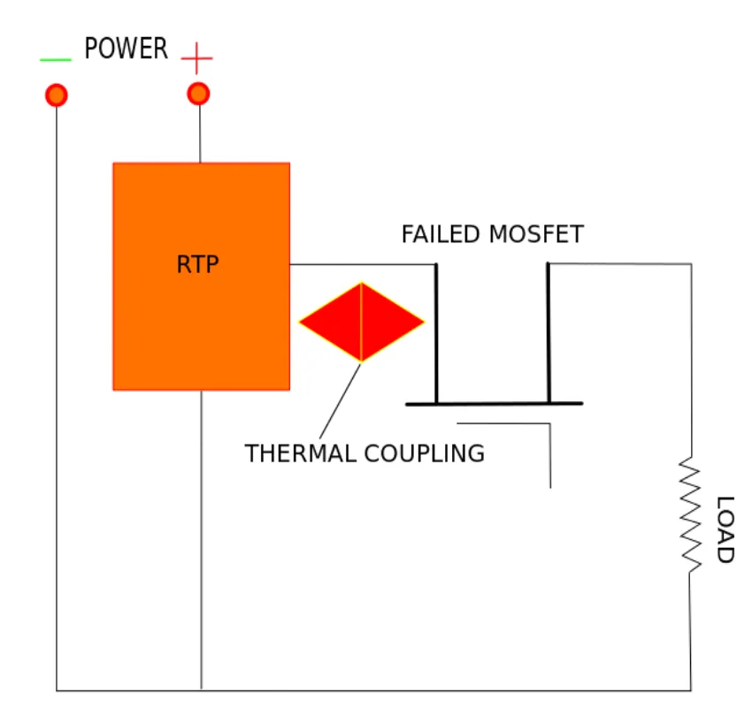
This figure is located in the “Learn from failure stories” section. It not only shows a failure state but, more importantly, introduces a protection concept. It reminds engineers that MOSFET switch design must consider not only normal operation but also anticipate failure modes and implement protections (like thermal protection), integrating reliability thinking into the design.
Most MOSFET failures do not involve sparks or smoke. They show up weeks later as intermittent resets, drifting sensor readings, or unexplained thermal hotspots.
A classic case: a designer selects a “large” MOSFET with an impressive current rating, then drives it directly from a 3.3 V GPIO. The device never reaches its specified low Rds(on), operating instead in a partially enhanced region. It works on the bench. In a warm enclosure, it slowly overheats.
Another frequent issue is ignoring Rds(on) altogether. At 600 mA, even 200 mΩ causes 72 mW of dissipation. In a SOT-23 package with limited copper, that is enough to raise junction temperature by several tens of degrees Celsius.
The pattern is consistent: the MOSFET was not actually used as a switch. It was unintentionally operated as a linear device.
How do you read MOSFET datasheets for switching use?
Focus on Vdss, Id, Rds(on), and package power dissipation
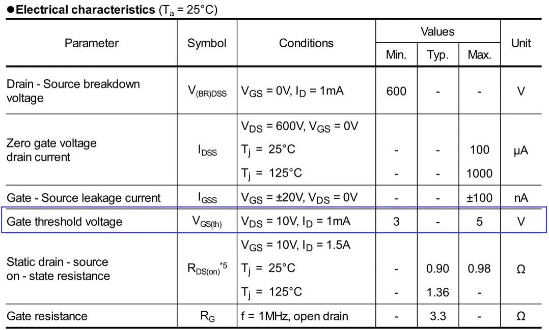
This figure is a core tool of the practical guide. It materializes the textual advice, showing a quick-reference sheet for “what to look for.” Through this real table, engineers can learn to ignore irrelevant information and directly locate key values that determine switching performance, loss, and safety margin, avoiding “datasheet phobia.”
MOSFET datasheets are dense, and many parameters are irrelevant for low-power switching. For most designs, four numbers matter more than everything else combined.
Vdss should include margin. A practical rule is at least 1.5× the supply voltage. For a 12 V rail, a 20–30 V device is a conservative baseline. This margin absorbs transients, ringing, and layout imperfections.
Id (continuous drain current) is frequently misunderstood. The headline value is usually specified at 25 °C with ideal thermal conditions. On a PCB, usable current is often a fraction of that number once temperature rise is considered.
Rds(on) is the dominant loss mechanism in low-voltage switching. Always verify the value at your actual gate drive voltage. A MOSFET advertised with “30 mΩ max” may only achieve that at 10 V Vgs. At 3.3 V, the real value could be several times higher.
Package dissipation and thermal resistance close the loop. A MOSFET with perfect electrical specs can still fail if the package cannot move heat into the board copper efficiently.
Interpret Vgs(th), logic-level specs, and gate charge (Qg)
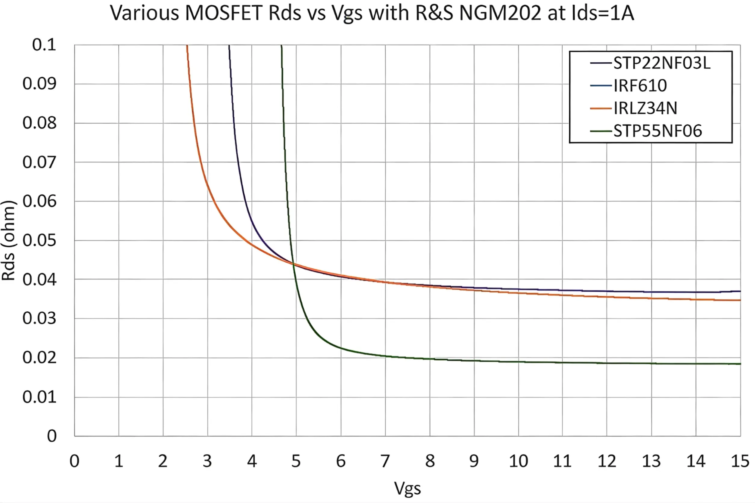
This figure provides graphical instruction on two of the most misunderstood parameters. It may contain curves or schematics to distinguish the gate voltage difference between “starting to conduct” and “fully conducting,” and to show the current demand of Qg during switching transients. This helps correct the misconception that “voltage above Vgs(th) is sufficient” and aids in understanding drive design for PWM or multi-MOSFET scenarios.
Vgs(th) causes more design mistakes than almost any other parameter. It does not indicate the voltage at which the MOSFET is suitable for switching. It marks the point where a tiny test current begins to flow—often a few hundred microamps.
For MCU designs, look for explicit logic level MOSFET data. That means Rds(on) values specified at 2.5 V, 3.3 V, or 5 V. If those curves or tables are missing, assume the device is not intended for direct GPIO drive.
Gate charge (Qg) determines how much current the MCU must supply during switching. At low frequencies, even relatively large Qg values are harmless. With fast PWM or many MOSFETs switching at once, total gate charge becomes a real load on the IO bank.
This topic overlaps with level-shifting and IO protection discussions. If your design goal is signal translation rather than load switching, it’s often better to use a dedicated approach, as discussed in this logic level shifter design guide.
Understand SOA curves and dV/dt limits for safe switching
The Safe Operating Area (SOA) defines combinations of voltage and current the MOSFET can survive without damage. While often ignored in low-power designs, SOA becomes critical during abnormal events: stalled motors, shorted loads, or slow gate transitions.
dV/dt limits and avalanche ratings matter whenever inductive loads are involved. Even a small relay coil can generate voltage spikes far beyond the nominal supply if energy is not properly managed. Many real-world MOSFET failures occur during turn-off, not steady conduction.
How should you choose between small-signal and power MOSFETs?
Map current and voltage ranges to MOSFET classes
One of the most common mistakes in mosfet as a switch designs is choosing parts by headline current ratings alone. The more reliable approach is to map voltage, current, and duty cycle together, not in isolation.
In most MCU-driven systems, small signal MOSFETs are well suited for loads up to roughly 1 A and supply voltages below 50 V, assuming reasonable duty cycles and proper layout. This includes indicator LEDs, sensor rails, small relays, and logic-controlled peripherals. Their advantages are compact packages, low gate charge, and simple drive requirements.
Once current climbs above 1 A—or when the load remains on for long periods—the thermal picture changes quickly. Even modest Rds(on) values can push dissipation beyond what SOT-23 or SOT-523 packages can safely handle. That is the point where power MOSFETs become less about “extra margin” and more about basic survivability.
A good illustration is the widely used BSS138. Electrically, it is rated around 50 V with a few hundred milliamps of drain current. In practice, it performs well as a small signal MOSFET switch for light loads or as part of level-shifting circuits. It is not intended for motors, fans, or loads with large inrush current. Treating it as such often leads to thermal drift rather than immediate failure—making the root cause harder to diagnose.
Compare packages: SOT-523, SOT-23, DFN vs DPAK, TO-220
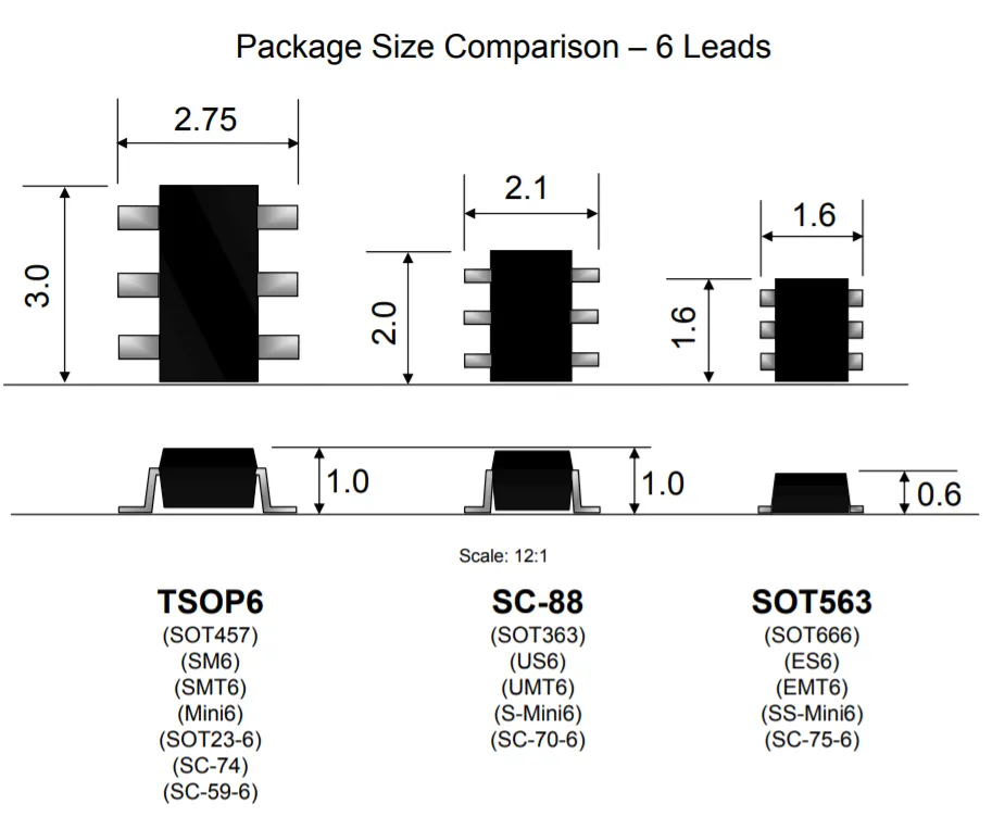
This figure links the abstract concepts of “thermal resistance” and “layout” to specific physical dimensions. It allows engineers to see at a glance that a MOSFET with “sufficient current rating” may have inadequate pad and copper area for heat dissipation on a real PCB if an overly small package is selected, thereby bringing the importance of thermal design forward to the selection stage.
Package selection is where many otherwise-correct designs quietly fall apart.
Tiny packages such as SOT-523 and SOT-23 rely almost entirely on PCB copper to remove heat. Without adequate copper area, even 50–100 mW of dissipation can cause a noticeable temperature rise. These packages shine when loads are light, switching is intermittent, and board space is tight.
DFN and LFPAK-style packages sit in a middle ground. With exposed pads and short thermal paths, they can dissipate several hundred milliwatts when paired with solid copper pours. For many low-voltage power rails, this is the most efficient compromise between size and robustness.
At the other end, DPAK and TO-220 packages offer enormous thermal headroom but at the cost of board area and assembly complexity. For small-signal switching, they are often unnecessary—unless the environment is harsh or fault conditions dominate the design constraints.
The key takeaway is simple: package choice should follow calculated dissipation, not intuition.
Decide between low-side N-channel and high-side P-channel switches
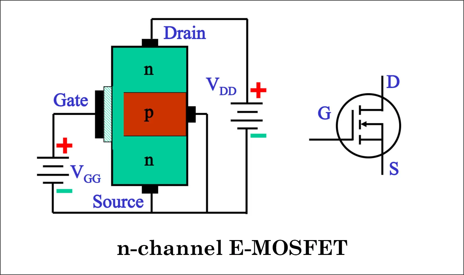
Low-side N-channel MOSFET switching remains the default for good reasons. Gate drive is straightforward, the source is tied to ground, and logic reference levels are clean. This simplicity reduces both schematic risk and firmware surprises.
High-side P-channel MOSFET switches, by contrast, keep the load grounded. This can simplify current sensing, reduce ground noise, or align with certain safety requirements. The trade-off is higher Rds(on) and reduced efficiency for the same silicon area.
In small-signal designs, the decision is usually architectural rather than electrical. If ground integrity and measurement simplicity matter more than a few tens of millivolts of drop, P-channel devices can still make sense. Otherwise, low-side N-channel switching remains the most forgiving option.
How do you design low-side MOSFET switches for MCU IO?
Sketch a basic low-side MOSFET switch topology
This figure is the “standard answer” illustration for handling inductive loads. It not only shows component connections but also emphasizes the energy reflux path (flyback diode) and the potential dangerous path (through the MOSFET’s body diode) via annotations. This figure is the foundation for understanding subsequent discussions on advanced protections like TVS diodes and SOA, emphasizing the necessity of anticipatory energy management in reliability design.
The canonical low-side MOSFET switch has changed very little over the years—and for good reason.
An MCU GPIO drives the gate through a small series resistor. The MOSFET source connects directly to ground. The drain connects to the load, which in turn connects to the supply rail. A high-value pull-down resistor on the gate ensures the MOSFET stays off during reset or boot.
Despite its simplicity, this topology is surprisingly resilient when designed with proper margins. Most failures trace back not to topology, but to parameter assumptions made too early in the design.
Size Rds(on) and estimate conduction loss for your load
This is where many designs either become robust—or quietly fragile.
Instead of guessing, engineers benefit from a small, repeatable selection framework. The table below represents a Small-Signal MOSFET Switch Selection Matrix that can be reused across projects.
| Application type | Vload V | I_load_max_A | Vdrop_allow_max_V | Rds_on_required_max_Ω | P_diss_required_max_W | Vdss_min_required_V | Package class | Thermal margin flag |
|---|---|---|---|---|---|---|---|---|
| LED rail | 5 | 0.2 | 0.1 | 0.50 | 0.02 | 7.5 | SOT-23 | PASS |
| Small relay coil | 12 | 0.08 | 0.2 | 2.50 | 0.016 | 18 | SOT-23 | PASS |
| Sensor power rail | 3.3 | 0.15 | 0.1 | 0.67 | 0.015 | 5 | SOT-523 | DERATE |
| Small DC fan | 12 | 0.6 | 0.2 | 0.33 | 0.12 | 18 | DFN | UPGRADE |
Core formulas used:
- Rds_on_required_max = Vdrop_allow_max / I_load_max
- P_diss_required_max = I_load_max² × Rds_on_required_max
- Vdss_min_required = 1.5 × V_load
Thermal interpretation follows a simple rule of thumb:
- ≤ 50% of package dissipation capability → PASS
- 50–80% → DERATE (layout or airflow matters)
- 80% → UPGRADE PACKAGE
This framework makes trade-offs visible early. It also explains why a part that looks acceptable electrically may still be a poor thermal fit.
Choose gate resistors and pull-down values for clean switching
Gate networks are often copied without thought, yet they strongly influence EMI and reliability.
A 10–100 Ω series gate resistor slows edge rates just enough to suppress ringing without materially increasing switching loss at low frequencies. In most small-signal applications, the exact value is not critical—as long as one exists.
A pull-down resistor around 100 kΩ prevents the gate from floating during reset or high-impedance MCU states. Skipping it often leads to confusing, intermittent behavior during power-up.
When multiple MOSFETs are driven from the same MCU bank, cumulative gate charge becomes relevant. In such cases, reviewing IO drive limits—or buffering critical gates—avoids subtle timing and stress issues. This topic intersects with IO protection strategies discussed in the reverse polarity and MOSFET protection guide, especially in mixed-voltage systems.
How do you protect MOSFET switches driving inductive loads?
Add flyback diodes for relays, solenoids, and DC motors
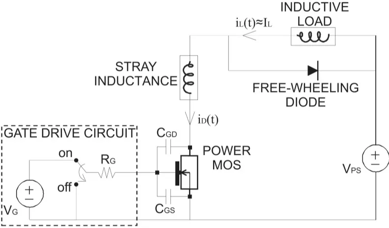
This figure is the technical core of the “How do you protect MOSFET switches driving inductive loads?” section. It not only marks the position of the “POWER MOS” device in the circuit but also, through labels like “INDUCTIVE LOAD”, “STRAY INDUCTANCE”, and “FREE-WHEELING DIODE”, fully reveals the physical process at the moment of turn-off: the continuity of load current forces energy to find a discharge path, and without the diode, the MOSFET’s drain would endure extremely high voltage stress. This figure visually demonstrates that in inductive load applications, the flyback diode is not an optional accessory but a necessary design component for ensuring the safe and reliable operation of the MOSFET.
The moment you hang an inductive load on a mosfet as a switch, you’ve signed an unwritten contract with physics. Current builds a magnetic field. Turn the switch off, and that field has to collapse somewhere.
If there is no defined path, the MOSFET becomes the path. Briefly. Violently.
That’s why flyback diodes are not “nice to have” parts. For relay coils, solenoids, and small DC motors, they are the difference between a predictable turn-off and a drain pin that sees far more voltage than anyone intended.
The diode choice itself is usually forgiving. Placement is not. Put the diode close to the inductive load, not just electrically connected somewhere on the board. Long loops radiate noise and inject spikes back into the supply, even if the diode exists on paper.
In low-speed applications—relays clicking a few times per second—this simple diode is often all you need. Problems start when designers assume “low power” automatically means “low risk.”
Combine flyback paths with TVS diodes in harsh environments
Some environments are simply less polite.
Automotive wiring, industrial cabinets, long cable harnesses—these systems inject fast transients that a flyback diode alone cannot tame. The diode handles energy release, but it is slow by nature.
This is where adding a TVS diode across the rail earns its keep. The TVS clamps the fast spike. The flyback diode deals with the stored energy. Each component does one job well, instead of one part being stretched beyond its comfort zone.
If you’ve ever seen a MOSFET survive bench tests but fail during vehicle testing, this is often the missing piece. The protection strategy described in this TVS diode selection guide applies directly here, even for “small” loads.
Respect SOA and avalanche ratings during fault events
Most switching circuits fail during faults, not normal operation.
A stalled motor, a jammed valve, or a shorted cable forces the MOSFET into regions where voltage and current overlap. This is exactly what the Safe Operating Area (SOA) warns about.
Avalanche ratings are not infinite shields. They describe what the silicon survives once or a few times—not what it tolerates repeatedly at elevated temperature. Designers who rely on avalanche as a routine operating mode often discover degradation long before outright failure.
For small signal MOSFET designs, conservative current limits and early voltage clamping are usually more effective than “heroic” silicon ratings.
How can you validate your MOSFET switch design on the bench?
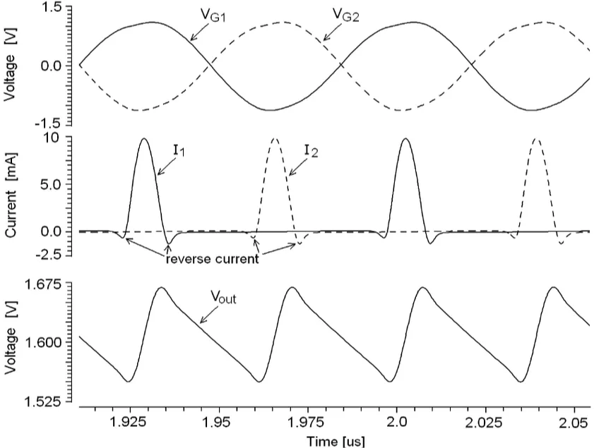
This figure is the bridge connecting design and testing, and the empirical conclusion of the entire article. It ultimately manifests all theoretical parameters (Qg, Rds(on), layout inductance) into measurable waveforms. Overshoot and ringing directly correspond to voltage stress and EMI; slow edges correspond to switching loss and thermal issues. This figure teaches engineers that final validation must rely on an oscilloscope, not just a logic analyzer or multimeter, thereby elevating the design from “connectivity” to the level of “signal integrity.”
Observe gate and drain waveforms with an oscilloscope
A multimeter will tell you whether the circuit works. An oscilloscope tells you whether it is healthy.
Look at the gate first. Are the edges clean? Too fast? Too slow? Then look at the drain. Overshoot and ringing are not academic details—they translate directly into EMI and stress.
One of the most effective fixes is also one of the simplest: adjusting the gate resistor. Moving from 10 Ω to 33 Ω or 47 Ω often calms a circuit dramatically, with negligible impact on switching loss at low frequencies.
This kind of tuning is far easier before layout is frozen.
Measure temperature rise under worst-case load and duty cycle
Thermal issues rarely show up at nominal conditions. They appear when everything stacks up: maximum load, maximum duty cycle, elevated ambient temperature.
Run the MOSFET exactly that way. Let it reach steady state. Then measure.
You do not need expensive tools. A thermocouple taped to the package is enough to expose optimistic assumptions. Compare measured temperature rise with a simple estimate:
ΔT ≈ P_diss × RθJA
If reality is worse than the math, copper area and layout—not the datasheet—are the usual culprits.
Build a repeatable incoming inspection checklist for MOSFET batches
As designs move toward production, variability matters.
Incoming inspection does not have to be elaborate. Check markings. Spot-measure Rds(on) at a known current. Perform a basic switching test with a standard load and watch temperature rise.
Many “mystery failures” are simply marginal parts slipping through without anyone noticing. Basic ESD discipline matters here as well; MOSFET gates remember abuse long after it happens.
How are small-signal MOSFET switches evolving in new designs?
Track market growth and new small-signal MOSFET families
Small signal MOSFET usage continues to grow steadily. The reasons are mundane rather than flashy: more connected devices, tighter power budgets, and increasing pressure to squeeze efficiency out of every rail.
What has changed is not topology, but predictability. Modern devices show tighter spreads in Rds(on), better characterization at low gate voltages, and more honest thermal data. That makes design outcomes less surprising.
Note innovations in low-voltage logic level MOSFETs for 1.8 V rails
As IO voltages slide downward, “logic level” no longer means 4.5 V.
Designers now expect meaningful Rds(on) performance at 2.5 V—and increasingly at 1.8 V. Parts that cannot meet this quietly fall out of favor, regardless of their legacy popularity.
The lesson is simple: always read the gate-voltage conditions attached to Rds(on). The number alone is meaningless without its context.
Watch wide-bandgap and high-integration switches for future upgrades
GaN and SiC dominate headlines, but mostly in high-voltage and high-power domains.
At the board level, silicon MOSFETs still offer the best balance of cost, availability, and simplicity for low-power switching. Integrated load switches are improving, but they trade transparency for convenience.
Many engineers still prefer discrete MOSFETs precisely because nothing is hidden.
What common mistakes break MOSFET switches in practice?
Why does my MOSFET get hot even with a “safe” current rating?
Why won’t my low-side N-channel MOSFET switch a high-side load correctly?
Can I use BSS138 or other small-signal MOSFETs for 12 V motors or fans?
Do I always need a flyback diode with a MOSFET switch and inductive loads?
How can one MOSFET circuit serve 3.3 V, 5 V, and 12 V loads safely?
Final note
A MOSFET as a switch rarely fails because the part was exotic or insufficient on paper. It fails because one assumption went unchallenged: gate voltage, thermal path, fault duration, or layout.
Designing with those assumptions exposed—and tested—turns a simple transistor into a reliable system element rather than a silent liability.
Bonfon Office Building, Longgang District, Shenzhen City, Guangdong Province, China

A China-based OEM/ODM RF communications supplier
Table of Contents
Owning your OEM/ODM/Private Label for Electronic Devices andComponents is now easier than ever.
