MMBT3904LT1G SOT-23 Transistor Guide
Nov 14,2025
Preface
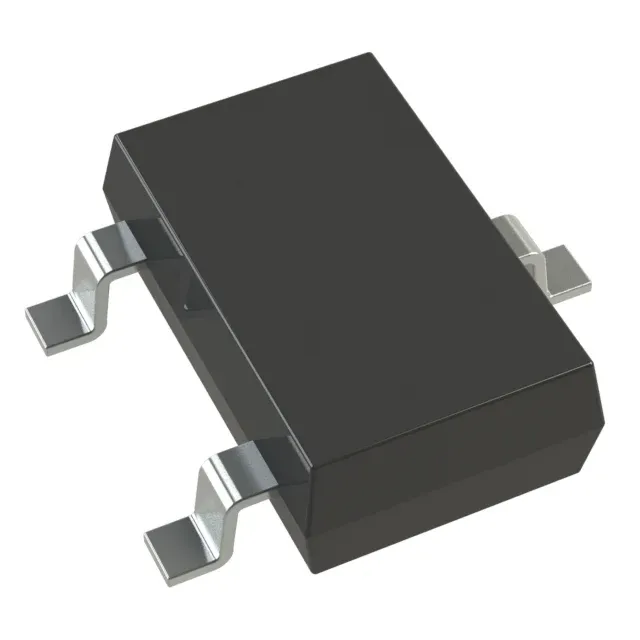
Ask any engineer to name their first transistor, and chances are it’s something like the MMBT3904LT1G—a tiny NPN BJT in a SOT-23-3 case that has powered countless test circuits, logic drivers, and LED indicators. It’s the kind of part you stop noticing after a while because it just works.
The reason it’s everywhere is simple: this small device delivers enough current headroom (up to 200 mA) and voltage tolerance (40 V VCEO) for most logic-level designs, while staying cool at only 300 mW dissipation on standard FR-4. Add RoHS 3 compliance, MSL 1 rating, and a wide –55 °C to +150 °C junction range, and you have a transistor that’s hard to break and easy to source.
Whether you’re building a breadboard prototype or a 10 000-unit production board, understanding its pinout, marking codes, and thermal behavior can save hours of debugging.
How do you identify MMBT3904LT1G fast—pinout, top mark, and package checks?
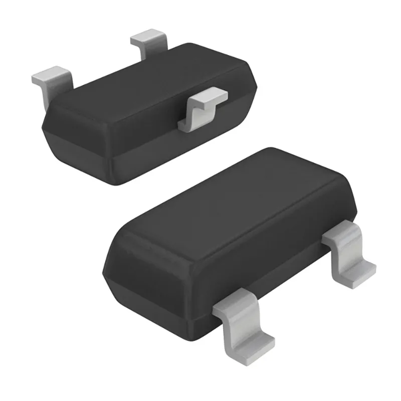
The figure pairs common reel/marking notes with the JEDEC TO-236-AB footprint so you can decode lots and drop the device into existing 2N3904-style layouts safely.
Under a microscope, one SOT-23 looks just like another—until it doesn’t. The MMBT3904LT1G, made by onsemi, often ships on reels marked “TR”, “CT”, or “Digi-Reel” depending on whether it’s factory tape or cut-tape from distributors such as DigiKey or Mouser.
It’s part of the discrete BJT transistor family (category: Bipolar, NPN), rated for:
- Collector current (IC max) = 200 mA
- Collector-emitter voltage (VCEO max) = 40 V
- Total power (Ptot) = 300 mW @ 25 °C
- Transition frequency (ft) ≈ 300 MHz
- Gain (hFE) ≥ 100 @ 10 mA, 1 V
and it keeps running happily anywhere between –55 °C and 150 °C TJ.
The standard SOT-23-3 (TO-236) footprint uses Pin 1 = Emitter, Pin 2 = Base, and Pin 3 = Collector.
That’s the same orientation you’ll find on most 2N3904 SMD layouts, so dropping it into an existing design is painless—as long as your schematic symbol doesn’t flip E and C. (That mix-up happens more often than people admit.)
Bench tip: When reviewing incoming reels, check the top laser code—usually “1AM” or “1A” with a faint G that simply means Pb-free plating. Don’t mistake it for a version code.
Decode the SOT-23 pins in 30 seconds (E–B–C orientation on common footprints)
The pad layout follows the JEDEC TO-236-AB standard: the emitter on the lower left, base lower right, collector top center. Leave at least 0.3 mm pad width and about 0.95 mm pitch to keep solder wetting balanced during reflow.
If you’re using a generic “SOT-23 transistor” symbol in OrCAD, KiCad, or Altium, double-check pin mapping. Several libraries reverse pins 1 and 3 by default—one of those gotchas that quietly breaks half your batch during bring-up.
Read the top-mark correctly (lot code vs Pb-free “G” note)
Markings on MMBT3904LT1G devices have evolved slightly across production years:
- 2015: onsemi switched to copper wire bonding (PCN Copper Wire Update 10 Sep 2015).
- 2018: added new wafer sources (Mult Dev Wafer Add 16 Nov 2018).
Both updates kept electrical behavior identical, so your simulation or SPICE model remains valid regardless of lot. RoHS 3 and MSL 1 classification also remained unchanged—no extra moisture bake needed before reflow.
If your QA process logs traceability, record both the reel label and laser code. It’s a small habit that simplifies cross-checking during failure analysis.
Choose a proper base resistor at 3.3 V / 5 V without over-saturating?
The 3-step method: target IC, pick forced β ≈ 10, compute Rb
- Decide your load current (IC): 20 mA for an LED, 50 mA for a relay coil.
- Force β ≈ 10: although hFE averages ≥ 100 @ 10 mA, designing for 10× base overdrive guarantees saturation.
- Calculate:
[ I_B = I_C / β_{\text{forced}},\quad
R_B = (V_{\text{drive}} − V_{BE(sat)}) / I_B ]
Example: 5 V logic driving 50 mA relay
to IB = 5 mA, VBE(sat) ≈ 0.9 V
to RB ≈ (5 – 0.9)/5 mA ≈ 820 Ω.
Using 820 Ω or 1 kΩ keeps the transistor cool and your MCU pin within limits.
| Parameter | Symbol | Typical Value | Design Note |
|---|---|---|---|
| Drive Voltage | Vdrive | 3.3 V / 5 V | MCU GPIO level |
| Load Voltage | Vload | e.g. LED 2.0 V | — |
| Collector Current | IC | 10-50 mA | Load setting |
| Forced Gain | β_forced | 10 | Hard-switch margin |
| VBE(sat) | ≈ 0.9 V | — | — |
| VCE(sat) @ 50 mA | ≈ 0.3 V | — | — |
| Base Resistor | Rb | ≈ (Vdrive − VBE)/IB | 470 Ω – 1 kΩ typ. |
| Power Loss (Ptrans) | ≈ VCE × IC | 15 mW @ 50 mA | Safe < 300 mW |
| Thermal Rise △T | RθJA ~ 556 °C/W | ≈8 °C @ 15 mW | Cool margin |
LED, small relay, logic-level loads: worked examples for 5–50 mA
| Application | Vdrive | IC | β_forced | Rb | Comment |
|---|---|---|---|---|---|
| LED Indicator | 3.3 V | 20 mA | 10 | ≈ 470 Ω | Pin draw ≈ 2 mA; clean saturation |
| Signal Relay | 5 V | 50 mA | 10 | ≈ 820 Ω to 1 kΩ | Add flyback diode (1N4148 or TVS) |
| Logic Inverter | 3.3 V | 5 mA | 10 | ≈ 220 Ω | Sharp edges for TTL input load |
Can MMBT3904LT1G handle my load current and power safely?
This part was never meant to drive motors, yet it holds its ground surprisingly well. The 200 mA IC limit, 40 V VCEO, and 300 mW Pd @ 25 °C give generous room for logic-level work.
In real PCBs, junction heating depends on copper area. A tiny 1 mm² pad can reach about RθJA ≈ 556 °C/W, meaning each 100 mW adds ≈ 55 °C rise. Double that pad size and you cut it nearly in half.
Example: Relay load 50 mA to VCE(sat) 0.3 V to P ≈ 15 mW to ΔT ≈ 8 °C.
Even at full 200 mA, 60 mW only raises ≈ 33 °C, leaving ample margin below TJ(max)=150 °C.
Quick checks: IC 200 mA / VCEO 40 V / Pd 300 mW @ 25 °C
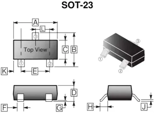
The figure highlights equal pad geometry and proper stencil openings to avoid skew/tombstoning, reflecting the guide’s practical reflow advice for SOT-23 parts.
| Parameter | Symbol | Rating | Design Comment |
|---|---|---|---|
| Collector-Emitter Voltage | VCEO | 40 V | Safe for low-voltage logic |
| Collector Current (DC) | IC | 200 mA | LEDs / Relays acceptable |
| Power Dissipation | Ptot | 300 mW @ 25 °C | Derate ≈ 2.4 mW/°C |
| DC Gain | hFE | ≥ 100 @ 10 mA | Design β ≈ 10 |
| Transition Frequency | ft | ≈ 300 MHz | Good for 3.3-5 V switching |
| Junction Temp Range | TJ | -55 ~ 150 °C | Industrial grade |
How does ft (≈300 MHz) and hFE spread impact 3.3 V / 5 V switching?
When engineers look at the MMBT3904LT1G datasheet, they often skip over the transition frequency and gain spread graphs. Yet those two lines quietly dictate how your logic edges behave. The part’s typical ft ≈ 300 MHz gives more than enough bandwidth for microcontroller-level switching; in other words, it won’t limit you at 3.3 V or 5 V.
But real parts vary. A production batch can show hFE anywhere between 100 and 300 at 10 mA / 1 V. At lower collector currents—say 1 mA—gain falls sharply, so small-signal stages or sensor pull-ups may need bias tweaks. That’s why you don’t design right at the edge; you choose a forced β ≈ 10 for saturation and forget the rest.
In fast GPIO drivers, the real performance bottleneck isn’t frequency, it’s charge removal from the base. Over-driving the base cuts switching delay, but too much charge leaves the transistor “sticky,” adding a few extra microseconds of tail current. When you see a lazy falling edge on your oscilloscope, that’s usually why.
Low-current gain pitfalls: read hFE @ 10 mA vs bias margin
Datasheets love quoting hFE = 100 @ 10 mA, but few designers actually drive that hard. If your circuit runs closer to 2 mA, expect a gain closer to 50–60. That means your 10 kΩ base resistor calculated for a 10 mA load may no longer saturate the device fully at low bias. It’s one reason LED strings sometimes glow unevenly at 3.3 V.
A good habit is to sweep the base resistor experimentally—start high, step down until VCE(sat) levels off. That “knee” marks true saturation. Doing this once on a breadboard teaches more than any equation.
When to avoid linear region and stay in hard saturation for GPIO drive
While the MMBT3904LT1G transistor can operate in linear mode for analog biasing, its sweet spot is fast digital switching. Keeping it in hard saturation reduces power loss (≈ VCE(sat) × IC = 15 mW typ @ 50 mA) and prevents thermal creep. Linear operation, by contrast, raises junction temperature fast because VCE floats above 1 V.
In digital designs, the rule is simple: either off or on. If you need mid-range control—like pulse-width modulation for LEDs—let a MOSFET take over. The MMBT3904LT1G is happiest flipping clean edges all day long.
Lay out and reflow with fewer failures—what footprint, stencil, and reflow limits matter?
A compact table of pad/stencil/reflow limits used to reduce rework and ensure solid fillets—especially where the collector pad ties to larger copper for heat spread.
You can tell a lot about a product line by how it survives reflow. The SOT-23 package of MMBT3904LT1G follows onsemi’s TO-236 outline, and it’s forgiving if you respect a few geometric truths.
First, pad balance. Keep your copper pads equal length (≈ 0.8 – 1.0 mm) and solder mask clearance around 0.05 mm. An unbalanced stencil opening can pull the part sideways during reflow—a phenomenon known as tombstoning.
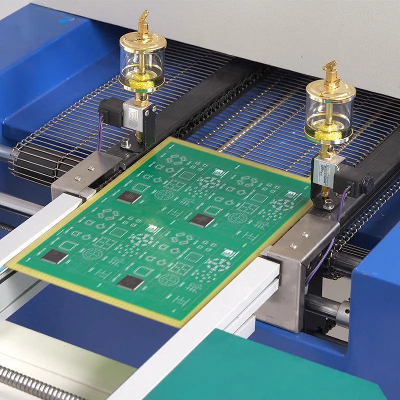
Second, thermal profile. The part is rated MSL 1 (unlimited floor life), which means you can store it open to air without pre-bake. Reflow peaks near 245–260 °C are fine, with soak time 60–120 s @ 150–200 °C. Stay below 260 °C for more than 10 s to preserve plating adhesion.
Assembly tip: When debugging joint cracks, look at stencil thickness first. A 0.125 mm (5 mil) stencil often yields smoother fillets than 0.15 mm when using SAC305 lead-free paste.
(Subtle mention: Reflow handling practices overlap with component selection notes in TEJTE’s TVS Diode Selection & Testing Guide, since both address ESD and solder stress reliability.)
SOT-23 pad sizes & solder cues—avoid skew during reflow
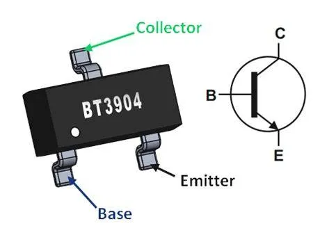
The figure mirrors the guide’s bench checks—sweeping IC for VCE(sat) and viewing 5 V/10 kHz edges—catching library pin swaps or solder issues without complex gear.
| Feature | Recommended Size / Limit | Why It Matters |
|---|---|---|
| Pad length | 0.8 – 1.0 mm | Controls solder wicking |
| Pad width | 0.3 – 0.4 mm | Ensures even wetting |
| Pitch (E-B) | 0.95 mm | Matches JEDEC TO-236-AB |
| Stencil thickness | 0.10 – 0.125 mm | Balanced solder volume |
| Peak reflow temp | 245 – 260 °C | Pb-free process window |
| MSL rating | 1 (Unlimited) | No bake required |
Observe MSL 1 and solder temperature limits during multiple reflows
Designers sometimes worry about double-sided boards going through two passes. Fortunately, the MMBT3904LT1G’s MSL 1 rating means it can handle that without pre-drying. Still, avoid exceeding total time-above-liquidus twice the spec; moisture isn’t the risk—copper diffusion is.
In rework situations, hot-air reflow around 250 °C for 10 s is safe. Go slower rather than hotter; these tiny devices cool quickly but plating layers don’t forget abuse.
Test it in minutes—what benches validate saturation, leakage, and switching speed?
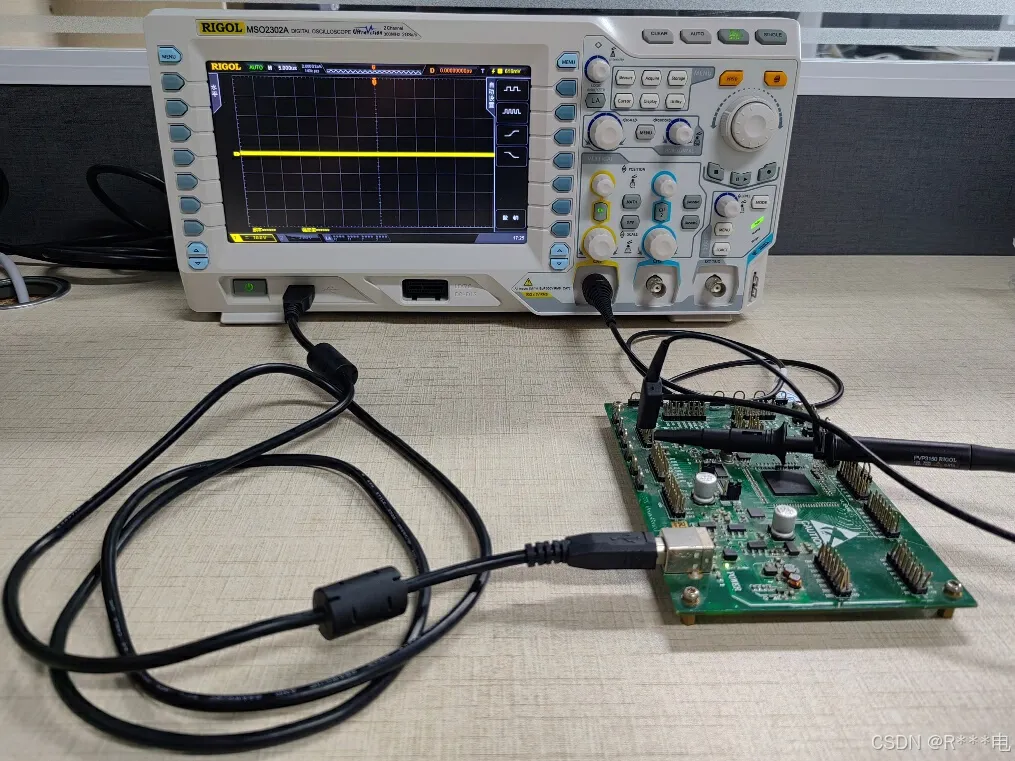
The image shows a practical test setup for MMBT3904LT1G: the device is soldered on a small PCB and driven from a source-measure unit while a digital oscilloscope captures rise/fall edges. Typical checks include VCE(sat) under a forced-β drive, DC gain consistency, leakage at room temperature, and waveform integrity at a moderate switching frequency—matching the guide’s validation flow before production use.
Bench testing this transistor doesn’t require fancy equipment. A basic breadboard setup with a function generator and oscilloscope tells nearly everything about a MMBT3904LT1G’s health.
Start with VCE(sat) measurement. Drive the base through a known resistor, sweep the collector load from 5 mA to 50 mA, and watch where voltage stops dropping. Typical curves line up with datasheet values—about 0.3 V @ 50 mA.
Next, check switching speed. Feed a 10 kHz square wave into the base via 1 kΩ, power the collector through 1 kΩ to 5 V, and view the collector waveform. Rise and fall edges around 100–150 ns show a healthy part. If they stretch beyond 300 ns, check the scope ground path or excessive base capacitance.
Simple scope tests: VCE(sat) vs IC sweep; rise/fall with 1 k–10 k drive
| Test | Setup | Expected Result |
|---|---|---|
| VCE(sat) curve | Sweep IC 5–50 mA @ VBE(sat) 0.9 V | ≈ 0.1–0.3 V range |
| Sweep IC 5–50 mA @ VBE(sat) 0.9 V | 5 V square input to 1 kΩ base resistor | 100-150 ns rise/fall |
| Leakage check | Reverse VCE = 30 V, base open | < 50 nA typ. |
| Thermal drift | Measure VBE @ 25 °C to 85 °C | ΔVBE ≈ –2 mV/°C |
ESD handling and basic protection hints
The MMBT3904LT1G is rugged but not invincible. Its base-emitter junction can break down near 6 – 7 V, which is fine for most logic lines but marginal if long cables or coils are involved. A small ESD diode at the connector side helps immensely.
When the transistor drives a relay or inductive load, always add a flyback diode (1N4148 or TVS SMBJ5.0A) near the coil. It suppresses voltage spikes that would otherwise punch through the junctions.
For higher-energy interfaces, reference TEJTE’s TVS Diode Selection & Testing Guide (5 V / 12 V / 24 V Matrix Explained) — it shows how transient suppressors extend transistor lifetime without extra series resistance.
Where to get the official datasheet, SPICE model, and EDA symbols quickly?
If you design more than once a month, you probably keep a small stash of reference models. The MMBT3904LT1G should be one of them. The onsemi official datasheet—MMBT, SMMBT3904L—is still the best reference for absolute ratings and switching curves.
You’ll find SPICE models and PCB footprints readily available across EDA ecosystems: LTspice, PSPICE, KiCad, and Cadence OrCAD libraries all list the SOT-23 version. In most cases, the symbol name is simply “MMBT3904” without the LT1G suffix. That suffix only identifies reel packaging and RoHS compliance, not electrical differences.
For layout, use the SOT-23-3 (TO-236) footprint, which aligns with standard transistor pads and thermal profile data already stored in KiCad’s Device library. Just confirm the pin mapping (1–E, 2–B, 3–C) before final routing—some open-source libraries reverse it.
Practical pointer: To save time, create a verified component entry linking schematic symbol, footprint, and SPICE file in your EDA tool once. It avoids future errors and streamlines simulation for LED or logic buffer circuits.
Datasheet & SPICE essentials checklist
| Resource Type | Source | Purpose / Tip |
|---|---|---|
| Datasheet | onsemi "MMBT, SMMBT3904L" | Main reference for Vceo, hFE, ft |
| SPICE Model | onsemi, LTspice default | For analog or switching simulation |
| EDA Symbol | Eagle / OrCAD / KiCad | SOT-23 footprint verified |
| PCB Library | JEDEC TO-236-AB | 0.95 mm pitch, 0.3 mm pad width |
| RoHS / REACH Data | onsemi RoHS Declaration | Confirms Pb-free (G) plating |
| PCN Archive | onsemi 2015 / 2018 | Wire bonding and wafer source updates |
Source with confidence—what changed in 2024–2025 that affects small-signal BJTs?
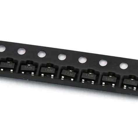
The image summarizes process consolidation, steady supply, and common packaging so production teams can pick TR for PnP or CT for prototyping with consistent top-marks.
The small-signal transistor market rarely makes headlines, but 2024 and 2025 brought subtle shifts that engineers should note. onsemi streamlined several low-power discrete lines, consolidating legacy part numbers under unified wafer processes. That means parts like the MMBT3904LT1G now share the same foundry flow as equivalents such as MMBT2222A or MMBT4401, improving yield consistency and reducing parameter drift.
Distributors like DigiKey, Mouser, and LCSC report steady supply—tape & reel formats (“TR”) dominate for automation, while cut tape (CT) and Digi-Reel are best for low-volume prototyping. Pricing in Q4 2025 typically ranges between $0.03–0.06 per unit in bulk reels, depending on region and packaging.
From a compliance standpoint, RoHS 3 and REACH remain satisfied. The component’s export classification, ECCN = EAR99, means no licensing burden for international shipments. For production teams, that’s one less paperwork headache.
Sourcing tip: Subscribe to onsemi’s PCN service if you rely on verified lots. Their 2025 updates note a tighter parametric binning for hFE, which helps avoid variation in analog designs.
Distributor snapshots and packaging insight
| Distributor | Format Options | Notes |
|---|---|---|
| DigiKey | Tape & Reel / Cut Tape | "LT1G" Pb-free suffix; ready stock |
| Mouser | Tape & Reel | Matches onsemi catalog revision |
| LCSC | Reel only | Good for Asia production runs |
| TEJTE internal stock | SOT-23 verified | Used for lab builds and case demos |
Build these practical circuits now—LED driver, inverter, debounce, and level-shift
3.3 V MCU to LED (10–20 mA)
Use the base-resistor formula from earlier:
Vdrive = 3.3 V, IC = 20 mA, βforced = 10, giving Rb ≈ 470 Ω.
Collector goes to the LED’s cathode; emitter to ground. This yields strong brightness without pulling more than 2 mA from the GPIO pin.
5 V GPIO to Mini Relay (flyback diode required)
TTL-style inverter or debounce circuit
FAQs
1. Where can I get a verified SPICE model for MMBT3904LT1G, and will it drop-in for LTspice or PSPICE?
Yes. The official onsemi model works in both tools without modification. Just match the SOT-23 pin numbering and define NPN MMBT3904 in your circuit.
2. What’s the safe way to size a base resistor from a 3.3 V MCU when driving 20–50 mA loads?
Follow the 3-step saturation method in this guide: choose β ≈ 10, compute IB = IC / β, then Rb = (Vdrive – VBE) / IB. Values between 470 Ω–1 kΩ cover most use cases.
3. How do I read SOT-23 top markings on MMBT3904LT1G and avoid QC confusion?
Laser code “1AM” or “1A” identifies the part; the trailing “G” means Pb-free. Different font thicknesses reflect batch differences, not electrical changes.
4. Is the MMBT3904LT1G footprint compatible with Eagle or OrCAD standard SOT-23?
Yes—use the JEDEC TO-236-AB template. Just ensure pins map correctly (1-E, 2-B, 3-C).
5. What reflow and handling limits apply if my board runs two passes?
Rated MSL 1, it withstands multiple reflows below 260 °C × 10 s per pass without moisture pre-bake.
6. How do distributor part options differ (Tape & Reel vs Cut Tape)?
Functionally identical. Choose TR for automated pick-and-place, CT for hand assembly.
7. Have there been any 2024–2025 updates from onsemi that might affect sourcing or documentation?
Yes—process consolidation and minor hFE bin tightening. Subscribe to onsemi PCN alerts to stay current.
Final Notes
Bonfon Office Building, Longgang District, Shenzhen City, Guangdong Province, China

A China-based OEM/ODM RF communications supplier
Table of Contents
Owning your OEM/ODM/Private Label for Electronic Devices andComponents is now easier than ever.
