MC34063 DC-DC Guide: Buck, Boost & Inverting
Dec 19,2025
Why This Tiny DC-DC Controller Still Matters

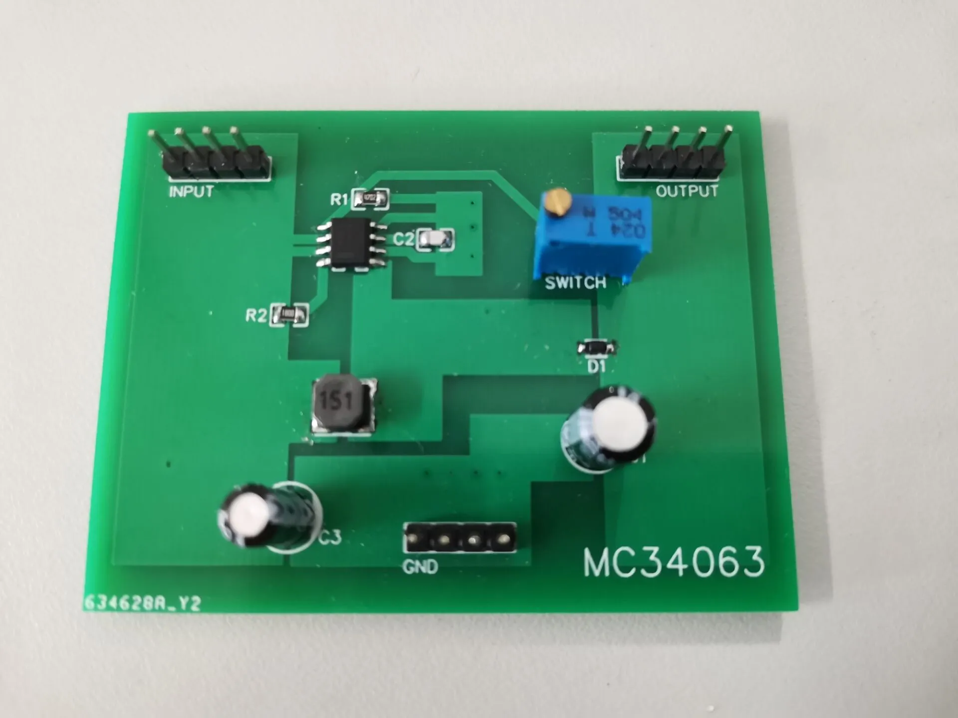
This graphic introduces the discussion of this classic chip, emphasizing its simplicity, reliability, and “hard to kill” nature. It symbolizes a design philosophy that enables building stable power supplies without complex simulations or exotic magnetics, but also hints at potential failures if design boundaries (like topology selection or inductor ripple) are ignored.
Few parts in the power-supply world have aged as gracefully as the TEJTE MC34063 DC-DC converter.
It’s a modest eight-pin IC that still ships by the millions, quietly regulating everything from router boards to automotive sensors. Despite new synchronous bucks and GaN-based regulators taking the spotlight, engineers continue to trust the MC34063 because it’s predictable, accessible, and hard to kill.
You don’t need simulation licenses or exotic magnetics to make it work. A bench supply, a scope, and a short parts list are enough to build a stable converter that runs for years. But this same simplicity can deceive: if you choose the wrong topology, ignore inductor ripple, or push the chip near its 1.5 A switch limit, it will oscillate, overheat, or fold back under load.
That’s why TEJTE built this practical guide—to help you size every component correctly, interpret the waveforms, and compare your real-world data against proven formulas. It’s written for people who care about both efficiency and reliability, not just making the LED turn on.
Which MC34063 topology fits your input and load?

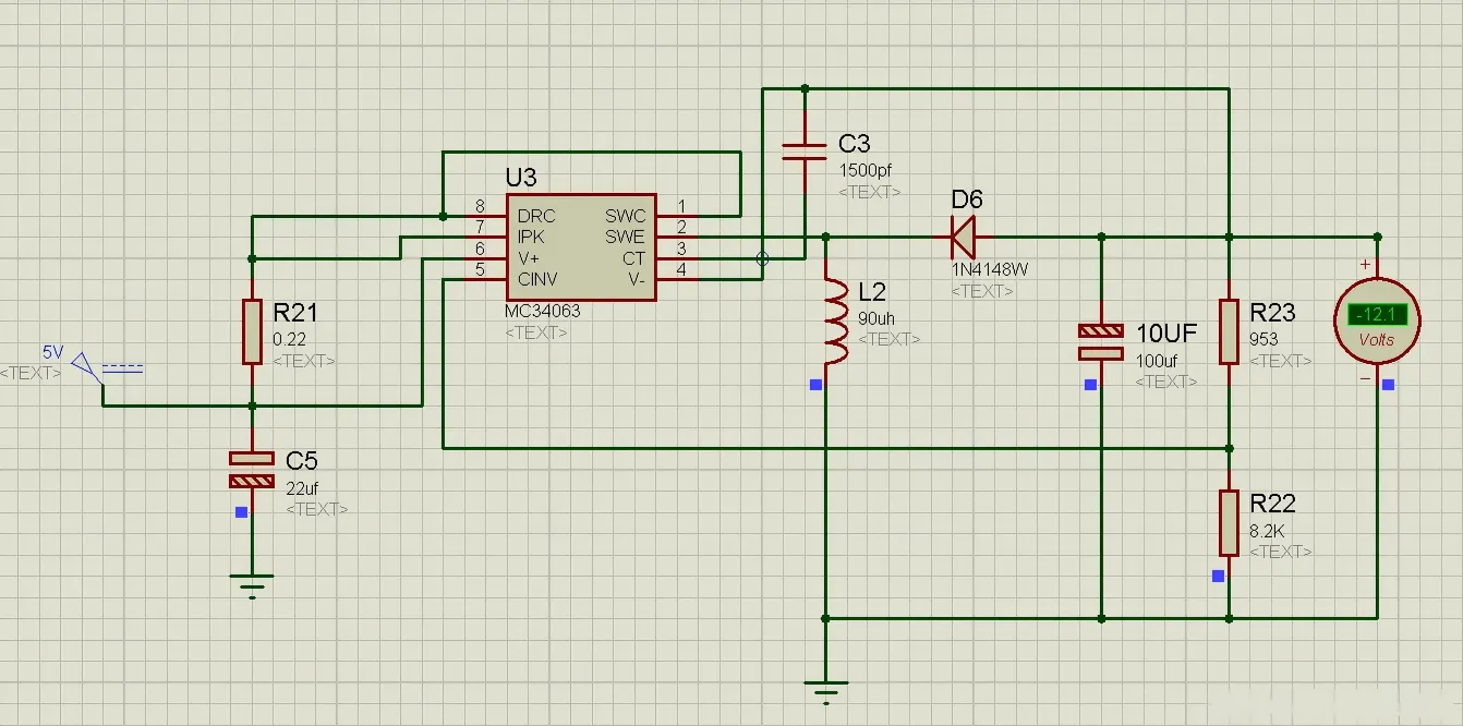
This schematic is the visual core for topology selection. It clearly indicates that the choice among topologies is not about preference but is strictly dictated by input/output voltage relationships and polarity requirements. The accompanying table further summarizes each topology’s input/output polarity, common conversion ranges, and typical uses, helping designers make the correct choice quickly and understand key electrical boundaries like duty cycle.
Decide between buck, boost, and inverting by VIN/VOUT range, polarity, and duty cycle
| Topology | Input Polarity | Output Polarity | Common Range | Typical Use |
|---|---|---|---|---|
| Buck | + | + | 12 V to 5 V / 9 V to 3.3 V | Logic rails or MCU power |
| Boost | + | + | 5 V to 12 V / 3.3 V to 9 V | Step-up from USB or Li-ion |
| Inverting | + | - | +12 V to -12 V | Analog or op-amp bias lines |
A good starting question is simple: Is your target voltage above or below the source?
If below to buck.
If above to boost.
If negative to inverting.
Experienced designers also watch the duty-cycle limits. With the TEJTE MC34063, you’ll want D > 0.2 in buck and D < 0.8 in boost to keep regulation tight and switching losses under control. Ignore those boundaries, and the converter can slip into discontinuous chaos—especially when your inductor value drifts out of spec.
Understand the electrical boundaries
Internally, the chip’s switch saturates near 0.8 V, which slightly eats into your voltage margin. For example, a 12 V to 5 V step-down running at 0.5 A will draw about:
[ I_{IN} ≈ \frac{V_{OUT} × I_{OUT}}{V_{IN} × η} = \frac{5 × 0.5}{12 × 0.72} ≈ 0.29 A ]
But that’s average current. Add ripple and transient spikes, and you’re close to 1 A peak—enough to test the limits of the internal switch. TEJTE recommends keeping at least 20 % headroom on both current and thermal dissipation for long-term stability.
In practice, that means pairing the controller with an inductor that has low DCR (<0.3 Ω) and a saturation current ≥ 1 A, along with a Schottky diode rated above your peak load. That alone prevents most first-prototype failures.
Can MC34063 step down 12 V to 5 V safely and efficiently?
Bill of materials for a proven 12 V to 5 V @ 0.5 A design
| Component | Typical Value | Selection Note |
|---|---|---|
| L1 | 220 μH | Keep DCR < 0.3 Ω; ≥ 1 A sat current |
| D1 | TEJTE SS14 Schottky | Low VF ≈ 0.45 V minimizes loss |
| RSC | 0.33 Ω | Limits switch current ≈ 0.9 A |
| Ct | 470 pF | Targets ≈ 100 kHz fSW |
| Cout | 470 μF / 25 V | ESR 0.1-0.3 Ω for stable loop |
| Cin | 100 μF / 0.1 μF ceramic | Bypasses high-frequency noise |
| Controller | TEJTE MC34063A (DIP-8) | Integrated 1.5 A switch |
How small parts make big efficiency gains
Three real-world tweaks can lift efficiency from 65 % toward 75 %—sometimes higher on short traces:
- Diode VF: every 0.1 V saved is roughly a 2 – 3 % efficiency boost.
- Inductor DCR: since copper loss scales with I²R, dropping from 0.5 Ω to 0.25 Ω can shave 0.25 W at 0.7 A RMS.
- Ripple window (ΔIL): too high causes heating and audible buzz; too low may stall startup.
When done correctly, a compact buck can maintain < 100 mV ripple on the 5 V rail—clean enough for digital logic, Wi-Fi modules, or MCU cores used in TEJTE’s IoT reference platforms. And while newer switching regulators offer higher efficiency, the MC34063 still wins on cost and repairability.
If your project involves mixed 12 V and 5 V domains—say a router or control gateway—you can even pair this converter with TEJTE’s ESD protection diode layout guide to harden the rail against spikes without extra ICs.
How to build a 5 V to 12 V boost with predictable margins?

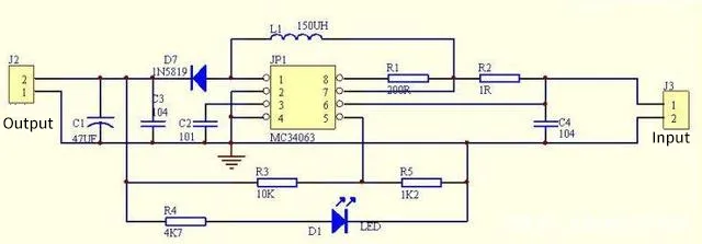
This schematic serves as a bridge from theory to practice, showing how to configure the MC34063 as a boost converter. It corresponds to the document’s discussion on the design challenges in boost mode, particularly the higher peak currents and stricter thermal management requirements. The component selections (e.g., using an SS34 Schottky diode) and layout hints provide a concrete reference for building a practical circuit with predictable margins.
Once you’ve mastered the buck, the boost converter feels natural—until you run into thermal headroom limits.
In this mode, the TEJTE MC34063 draws higher peak current and sees sharper switching spikes. That means every parameter—RSC, inductor, diode, and layout—matters twice as much as in step-down designs.
Bill of materials (boost @ 0.25 A) and thermal headroom
| Component | Typical Value | Design Note |
|---|---|---|
| L1 | 330 μH | Low DCR ≤ 0.4 Ω, ≥ 1 A sat current |
| D1 | TEJTE SS34 Schottky | 3 A IF rating; VF ≈ 0.45 V @ 1 A |
| RSC | 0.27 Ω | Sets current limit ~ 1.1 A pk |
| Ct | 470 pF | ≈ 100 kHz switching |
| Cout | 470 μF / 25 V | ESR ≤ 0.25 Ω for stability |
| Cin | 220 μF / 0.1 μF | Smooths high di/dt |
| Controller | TEJTE MC34063A SMD | Compact SOP-8 footprint option |
In a typical 5 V to 12 V @ 0.25 A build, the input current easily exceeds 0.7 A, and peak switch current can cross 1 A.
That’s close to the chip’s internal limit, so component derating and board cooling become non-negotiable. TEJTE recommends keeping total loss < 0.7 W for stable thermal behavior at ambient up to 60 °C.
Pro tip from TEJTE labs: never mount the MC34063 flush to copper pours without thermal vias underneath—this traps heat. A simple 3×3 mm pad array drops junction temperature by 6–8 °C.
Peak currents and RSC sizing caveats at high duty cycle

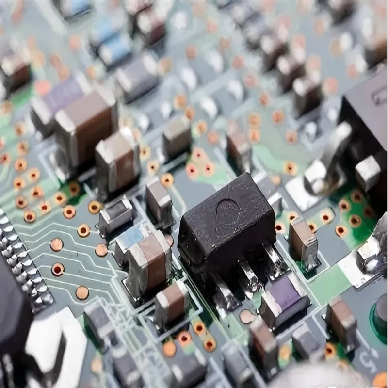
This graphic delves into the core challenge of MC34063 boost design—current control. It visually explains why special attention must be paid to RSC selection at high duty cycles and how improper calculation can lead to switch overheating or failure. The provided formulas echo the “Quick Calculator” section of the document, emphasizing the importance of rigorous calculation before finalizing the Bill of Materials (BOM), a critical step to prevent designs from operating on the edge of failure.
At high duty cycles (D > 0.7), the inductor peak current rises fast.
The sense resistor RSC controls this by setting a switch-current threshold of roughly 0.3 V / RSC.
[ I_{pk,limit} ≈ \frac{0.3}{R_{SC}} ]
So for RSC = 0.27 Ω, the limit is ≈ 1.11 A pk.
Add 20 % margin to cover component tolerances and inductor ripple:
[ I_{pk,total} ≈ I_{out} × \frac{V_{out}}{V_{in} × η} × \frac{1}{1 − D} + \frac{ΔI_L}{2} ]
For our example (5 V to 12 V @ 0.25 A, η ≈ 0.7, D ≈ 0.6, ΔIL ≈ 0.2 A):
[ I_{pk,total} ≈ 0.25 × \frac{12}{5 × 0.7} × \frac{1}{0.4} + 0.1 ≈ 1.08 A ]
That’s right on the edge — and exactly why TEJTE advises designers to confirm with the calculator before finalizing the BOM.
If you see the switch heating up too fast at light load, you’re likely running into reverse-recovery loss in the diode or a loop-area issue. Shorter traces help more than bigger caps.
Size the inductor, Ct, and RSC without guesswork
The following MC34063 Quick Calculator is a TEJTE in-house toolset—useful for both buck and boost modes.
All formulas are dimensionally consistent and follow tested bench data from TEJTE’s converter series.
MC34063 Quick Calculator
| Parameter | Formula | Notes / Units |
|---|---|---|
| Buck Duty Cycle (D) | D ≈ (Vout + VF) / (Vin – Vsat) | For 12 V to 5 V, D ≈ 0.46 |
| Buck Inductor (L) | L ≈ (Vin – Vout – Vsat) × D / (ΔIL × fSW) | ΔIL = 20–40 % of I out |
| Buck Peak Current (Ipk) | Ipk ≈ Iout + ΔIL / 2 | Used for RSC limit |
| RSC (sense resistor) | RSC ≈ 0.3 V / Ipk,limit | 0.3 V internal threshold |
| Boost Duty Cycle (D) | D ≈ 1 – (Vin – Vsat) / (Vout + VF) | For 5 V to 12 V, D ≈ 0.58 |
| Boost Inductor (L) | L ≈ Vin × D / (ΔIL × fSW) | ΔIL ≈ 25 % of I out |
| Switch Peak (Ipk) | Ipk ≥ Iout × (Vout / (η × Vin)) × (1 / (1 – D)) + ΔIL / 2 | Compare with device limit |
| Timing Cap (Ct) | fSW ≈ 1 / (4 × RT × CT) | Target ≈ 100 kHz |
Worked examples
Example 1 — 12 V to 5 V buck @ 0.5 A
( D ≈ 0.46 ), ( L ≈ 180 µH ), ( Ipk ≈ 0.55 A ), ( RSC ≈ 0.54 Ω )
Estimated efficiency ≈ 73 % with TEJTE SS14 diode.
Example 2 — 5 V to 12 V boost @ 0.25 A
( D ≈ 0.58 ), ( L ≈ 330 µH ), ( Ipk ≈ 1.08 A ), ( RSC ≈ 0.28 Ω )
Typical efficiency ≈ 70 %, depending on PCB loss.
These numbers are validated by TEJTE’s internal lab prototypes and mirror public results found on engineer forums and calculation tools like nomad.ee.
Still, always verify with your own scope—because switching noise and layout dominate the real world.
What layout rules prevent noise and oscillation on MC34063 boards?
This is where most DIY designs fail. A perfect calculation won’t save a noisy layout.
The TEJTE MC34063 behaves predictably only if the current loops are tight and the ground returns are short.
Core layout principles
- Keep the high di/dt loop (switch, diode, inductor, input cap) under 2 cm trace length.
- Place Cin (100 µF + 0.1 µF) right beside pin 6 (Vin) and pin 2 (GND).
- Use star grounding to separate power and signal grounds; connect at one node near RSC.
- Route feedback away from the switch node (pin 2 to pin 5).
- If oscillation appears on Cout, add a small RC snubber (10 Ω + 470 pF) across the switch.
ESR realities and stability tips
Output capacitor ESR (0.1–0.3 Ω) is part of the control loop — too low can make it unstable.
That’s why TEJTE still recommends electrolytics over pure ceramics for MC34063-based designs.
You’ll often see a sweet spot around 470 µF with ≈ 0.2 Ω ESR.
From the bench: on TEJTE’s boost evaluation board, replacing a 470 µF electrolytic with a 47 µF MLCC cut ripple by 30 %, but caused unstable ringing during load steps. Always validate on hardware — simulations can’t capture loop delay and diode recovery.
Validate your design: what should you measure first?
After assembly, don’t rush to load testing.
Start with waveforms and thermal behavior—your scope is the truth detector.
Scope the inductor ripple, diode recovery, switch saturation
- Probe the switch pin and inductor with short ground leads.
- Verify ripple is triangular and clean (no ring > 20 mV).
- Check the switch VCE(sat) ≈ 0.8 V — if it’s > 1 V, your RSC may be too low.
- Measure reverse recovery on the Schottky: spike < 20 ns is ideal.
Then compare your calculated values with a known reference like the TEJTE MC34063 Quick Calculator or public tools such as Nomad.ee.
If numbers diverge by > 15 %, look at layout inductance and scope grounding before blaming the formula.
When should you not use MC34063 and pick a modern regulator instead?
The TEJTE MC34063 is a legend, but not a miracle worker.
It’s ideal for cost-sensitive, low-power, or legacy maintenance projects—but once you start chasing high efficiency, tight EMI limits, or compact footprints, you’ll hit its natural ceiling.
Efficiency and EMI limits
Because it uses a bipolar transistor switch, not a MOSFET, the typical efficiency lands between 65–78%.
That’s perfectly fine for 0.5 A rails or backup supplies, but not for today’s 90%+ designs.
The switching frequency, around 100 kHz, also means larger inductors and capacitors compared to modern synchronous bucks running at 500 kHz–2 MHz.
If your product must pass CISPR Class B or automotive EMI, you’ll spend more time debugging than designing. In those cases, TEJTE engineers often recommend upgrading to synchronous DC-DC converters, such as the company’s newer low-EMI buck modules. They integrate MOSFETs, compensation, and soft-start—removing most layout headaches altogether.
Application trade-offs
Use MC34063 if you need:
- A simple, low-cost, field-repairable power stage.
- Wide VIN range (3 V–40 V) for mixed-voltage systems.
- Stable 5 V or ±12 V rails for control logic or instrumentation.
Skip it if you require:
- >85 % efficiency, especially above 1 A output.
- Tiny footprints or low ripple for high-speed ADCs.
- Strict EMC compliance or thermal constraints below 50 °C ambient.
In TEJTE’s internal projects, engineers now mix both worlds—using MC34063 for standby or auxiliary rails and synchronous bucks for high-efficiency loads.
That hybrid approach often saves cost without risking performance, especially when combined with TEJTE surge protection designs for 24 V industrial lines.
Industry pulse — DC-DC converter trends in 2025
Even as modern power ICs flood the market, the demand for low-cost DC-DC converters like MC34063 remains surprisingly strong.
According to industry research from 2024–2025, the global DC-DC converter market continues to grow at >10 % CAGR, driven by IoT, automotive, and telecom sectors.
The shift toward GaN and synchronous topologies is accelerating, yet legacy controllers stay relevant for maintenance, education, and rugged low-frequency systems.
TEJTE’s perspective aligns with this: keep producing reliable analog regulators for field engineers who need replacement parts or simple circuits that “just work.”
That’s why the MC34063 still appears in new designs—testing rigs, LED controllers, and hobbyist kits—despite its 1980s origin. The lesson? In engineering, mature doesn’t mean obsolete; it means proven.
FAQ: Solve the last-mile doubts before ordering
1. Is MC34063 good for 12 V to 5 V at 0.5 A in continuous duty?
2. How do I choose the inductor’s DCR and saturation rating?
Start by limiting ripple current to 20–40 % of Iout.
Then pick a core that stays unsaturated 20 % above Ipk.
DCR under 0.3 Ω is ideal for both buck and boost converters; higher values waste heat and reduce efficiency.
3. How can I estimate output ripple accurately?
Ripple ≈ (ΔIL × ESR + ΔQ/Cout).
For a 470 µF cap with 0.2 Ω ESR and 0.2 A ripple, you’ll see about 40 mV p-p.
Always confirm with a low-inductance probe tip at the output pin—long ground leads distort readings.
4. What fails first under surge or brownout conditions?
Usually the sense resistor (RSC) or inductor saturates before the switch transistor.
To improve robustness, TEJTE suggests adding a TVS diode on the input rail and a ferrite bead in series with VIN—exactly as outlined in their surge protection design notes for 24-V I/O systems.
Do this next: verify, prototype, and iterate
Theory is only half the battle.
Feed your VIN, VOUT, and IOUT into the TEJTE MC34063 Quick Calculator, grab your component shortlist, and breadboard it.
Scope the waveforms, tweak the inductor, and see if your ripple matches predictions.
That’s how every TEJTE power-supply engineer learns—by trusting the math, then verifying in copper.
Once the prototype is stable, freeze your Bill of Materials, order small batches from TEJTE’s authorized store, and document the exact parameters.
Future revisions are far easier when every value—Ct, L, RSC, and diode type—is written down and traceable.
And if you later migrate to a modern switching regulator, you’ll already have a strong baseline for comparison: efficiency, noise, and thermal curves from your MC34063 build.
Final note — building reliable DC-DC systems with TEJTE
Power electronics isn’t about perfection—it’s about predictability.
The MC34063 DC-DC converter remains the ultimate training ground for mastering buck, boost, and inverting topologies.
By following TEJTE’s practical sizing methods, observing clean layout habits, and validating each stage on real hardware, you can achieve a converter that performs reliably across temperature, load, and time.
Whether you’re designing an IoT sensor, a 12 V logic rail, or maintaining an industrial control unit, the combination of MC34063 simplicity and TEJTE engineering guidance gives you both understanding and control—a blend few modern chips can offer.
(For deeper study, see TEJTE’s guides on TVS diode layout for high-speed interfaces and surge protection in 24-V I/O systems, both directly complementing this DC-DC converter design.)
Bonfon Office Building, Longgang District, Shenzhen City, Guangdong Province, China

A China-based OEM/ODM RF communications supplier
Table of Contents
Owning your OEM/ODM/Private Label for Electronic Devices andComponents is now easier than ever.
