Logic Level Shifter Guide for I2C & MCU IO
Jan 4,2026
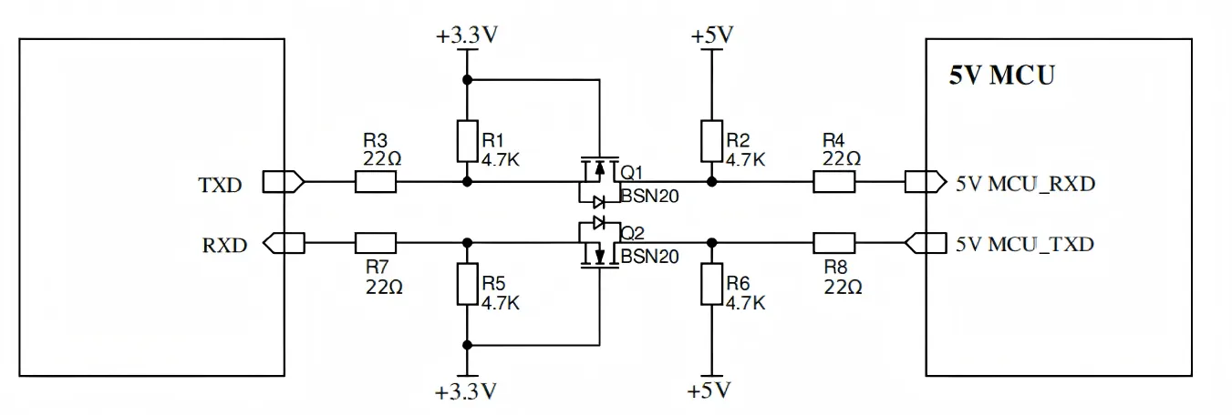
Located at the beginning of the article, this figure serves as an introduction, visually presenting the basic role of a level shifter when connecting devices at different voltages (e.g., a 3.3V MCU and a 5V sensor). It aims to establish the first impression: this is a common and inconspicuous component that, if mishandled, can cause hidden failures.
A logic level shifter usually doesn’t look dangerous on a schematic. It’s small, cheap, and familiar. Many engineers add it late, once the MCU, sensors, and connectors are already locked in. Nothing about it feels like a high-risk decision.
And yet, in mixed-voltage systems, that quiet little circuit often decides whether a digital bus behaves cleanly for years—or slowly turns unreliable after deployment. As MCU IO voltages keep dropping while 5 V hardware refuses to disappear, level shifting has become part of everyday embedded design, not a corner case.
This guide focuses on how level shifters behave in real I2C and MCU IO designs, where margins are finite and assumptions tend to come back later.
Why do you need a logic level shifter between 3.3 V and 5 V?
Understand voltage limits of 3.3 V MCUs and sensors
Most 3.3 V microcontrollers draw a very clear boundary around their GPIO pins. Absolute maximum ratings typically sit at VDD + 0.3 V. Cross that boundary and internal protection structures start to conduct. Those structures are meant to absorb short transients, not continuous current during normal operation.
This is not abstract theory. The behavior comes directly from how CMOS input stages and parasitic devices inside a MOSFET structure behave once voltage limits are exceeded, a mechanism commonly described in general semiconductor device discussions such as the standard explanation of how a MOSFET operates internally.
The problem shows up immediately when a 5 V device shares a digital interface with a 3.3 V MCU or sensor. Even if the overvoltage only occurs during logic highs, repeated stress slowly degrades the input stage.
Risks of direct 5 V-to-3.3 V connections
Direct connections are deceptive. On the bench, at low speeds and short trace lengths, everything often looks fine. Signals toggle. Data moves. Nothing overheats.
Months later, problems start appearing. An I2C bus occasionally misses an ACK. A peripheral fails only after a warm restart. A line sometimes refuses to release from low. These are classic symptoms of reduced electrical margin rather than outright damage.
What makes these failures painful is their inconsistency. They depend on temperature, supply tolerance, and device aging. By the time they surface, the design has usually shipped. From a reliability standpoint, skipping a logic level shifter introduces the same kind of hidden risk as skipping proper IO protection.
Typical use cases engineers actually run into
Mixed-voltage buses are everywhere. A 5 V controller talking to a 3.3 V IMU. A 3.3 V MCU interfacing with a legacy 5 V display module. Internal logic at 1.8 V connected to external headers expected to tolerate higher swings.
I2C deserves special attention because it is an open-drain bus. No device actively drives a logic high. Pull-up resistors define the high level instead. Without a 3.3 V to 5 V level shifter, the higher-voltage pull-up simply wins, pulling the entire bus above what the lower-voltage device is rated to tolerate.
This behavior is not an implementation detail. It follows directly from how the bus is defined in the official I²C-bus specification, which assumes open-drain drivers and external pull-ups.
When “5 V tolerant IO” really lets you skip it
Some MCUs advertise 5 V-tolerant input pins. In narrow cases, that claim is valid—but the conditions matter. Tolerance usually applies only when the pin is configured strictly as an input. Outputs still drive to VDD. Bidirectional buses remain unsafe.
There are often additional caveats. Internal pull-ups may need to be disabled. Tolerance may not apply during reset or power-down. Injected current limits still exist. If the datasheet does not state tolerance unambiguously for all operating modes, assuming it is safe becomes a gamble. In practice, adding a level shifter is often the simpler choice.
Compare common logic level shifter topologies for digital buses
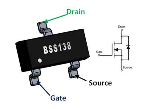
This figure is located in the chapter introducing the “resistor divider” topology. It provides a concrete, simple circuit example to illustrate the first level-shifting solution. At the same time, its simplicity sets the stage for explaining the limitations of this approach (e.g., unusable for bidirectional buses, increased source impedance) later in the text.
Use a resistor divider for simple one-way logic translation
Resistor dividers are the simplest tool available. Two resistors scale a 5 V signal down to something a 3.3 V input can survive. For slow, unidirectional signals—reset lines, enable pins, chip-select inputs—they can work acceptably.
Their limitations show up quickly on shared buses. Dividers increase source impedance, slow edges, and interact poorly with capacitance. They also fail completely for bidirectional signaling, which immediately rules them out for I2C.
Build a MOSFET-based bidirectional level shifter with BSS138
The MOSFET-based bidirectional level shifter exists for a reason. A small N-channel MOSFET and pull-up resistors on both sides create a circuit that naturally follows signal direction.
When either side pulls the line low, the MOSFET conducts and propagates the low across voltage domains. When the line is released, each side rises to its local supply. No direction control. No timing logic. Just physics doing what it naturally does.
This behavior aligns almost perfectly with open-drain buses like I2C, which is why the topology appears in countless application notes and reference designs.
Evaluate integrated logic level converter ICs vs discrete MOSFETs
Integrated logic level converter ICs offer capabilities discrete solutions cannot. Some control edge rates. Others handle push-pull signaling cleanly or support higher data rates.
The tradeoff is complexity. These ICs are less forgiving about layout, decoupling, and protocol assumptions. For many standard-mode and fast-mode I2C designs, a discrete MOSFET solution delivers the same functional result with fewer constraints.
Match topology to how the bus actually behaves
This is where many designs quietly go wrong. The topology must match the signaling style:
- I2C and one-wire: MOSFET translators or I2C-specific ICs
- SPI and UART: Direction-controlled buffers or unidirectional shifters
- Simple GPIO: Dividers or basic buffers
Using an I2C MOSFET shifter on a push-pull bus often “almost works,” which is usually worse than failing outright.
Choose between MOSFET, IC, and resistor level shifters for your bus
Decide based on bus speed, fan-out, and capacitance
Bus speed sets the rise-time target. Bus capacitance—trace length, connectors, device inputs—defines how hard that target is to meet. As capacitance increases, pull-up resistors must shrink, increasing sink current.
MOSFET-based shifters handle this tradeoff well at moderate speeds. As speeds climb and margins tighten, integrated solutions become more attractive.
Decide based on direction: unidirectional vs bidirectional
Balance BOM cost, board area, and assembly effort
When it’s time to move beyond BSS138-style solutions
How does a BSS138 level shifter circuit actually work?
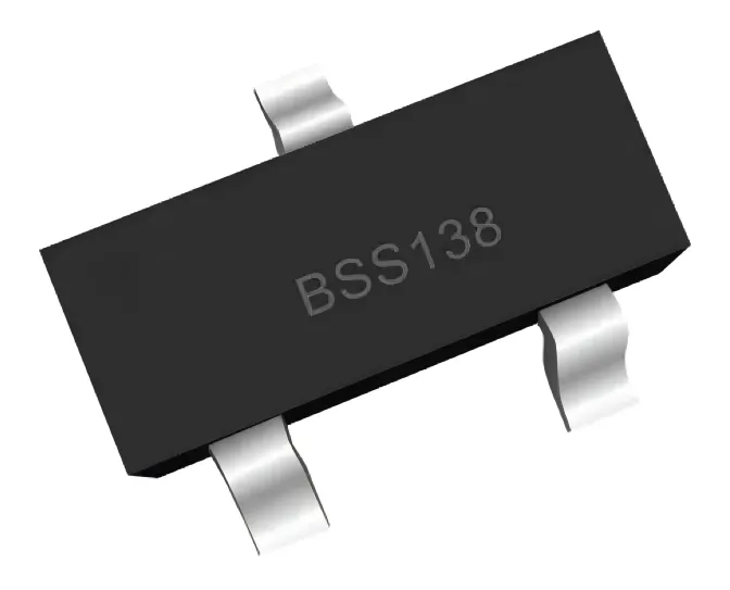
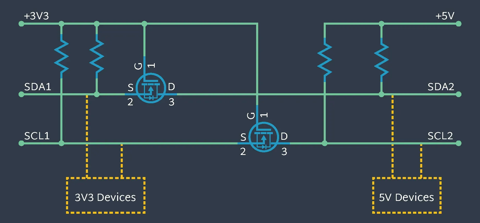
This figure is the core illustration for discussing the MOSFET solution. It first confirms the device symbol of the BSS138, then places it in a simplified application circuit. This helps readers connect the abstract “MOSFET solution” with a concrete, implementable circuit, laying the groundwork for the subsequent in-depth analysis of its working principle (e.g., the body diode conduction process).
Read key small-signal MOSFET parameters in the BSS138 datasheet
At first glance, BSS138 looks excessive for logic translation. It is an N-channel MOSFET rated for tens of volts and hundreds of milliamps—far beyond what an I2C line will ever demand. That apparent overkill is precisely why it behaves so predictably in level-shifting applications.
Several parameters matter more than the headline ratings. Vgs(max) defines how much gate stress the device can tolerate when rails are miswired or sequencing goes wrong. Rds(on) determines how firmly the MOSFET pulls a line low once it turns on. In practice, that resistance is tiny compared to typical pull-up values, so it has little impact on the bus low level. Gate charge (Qg) limits how quickly the device can respond, and at I2C speeds it is comfortably small.
All of this behavior traces back to basic MOSFET physics—how a conductive channel forms once Vgs exceeds threshold, and how parasitic structures behave during transitions. Those mechanisms are the same ones described in standard semiconductor explanations of how a MOSFET operates, which is why the circuit remains stable across a wide range of supply voltages.
Package size plays a secondary role. In tiny packages, thermal performance depends more on copper area than silicon limits. Fortunately, I2C currents are so low that thermal margins are rarely the limiting factor.
Follow current flow in the classic BSS138 I2C level shifter circuit
The elegance of the BSS138 level shifter comes from how well it matches open-drain signaling. Each side of the bus has its own pull-up resistor tied to its local supply. The MOSFET gate is referenced to the lower-voltage side.
When both sides idle high, the MOSFET remains off. Each bus floats to its own rail. Nothing unusual happens.
When the lower-voltage side pulls the line low, the source voltage drops. Vgs rises above threshold, the MOSFET turns on, and the low level propagates to the higher-voltage side. When the higher-voltage side initiates the low, the body diode conducts briefly, pulling the lower side down just enough to raise Vgs and turn the channel on. After that, the channel—not the diode—carries the current.
That brief body-diode conduction is intentional, not a flaw. It is what allows the circuit to work bidirectionally without direction control. This behavior aligns exactly with the open-drain assumptions defined in the official I²C-bus specification.
Once both sides release the line, the MOSFET turns off again, and each side rises independently through its pull-up.
Check safe operating limits for common voltage pairs
In real designs, the BSS138 topology works comfortably for 1.8 V to 3.3 V and 3.3 V to 5 V translation. Voltage rating is rarely the constraint. Signal integrity is.
As voltage gaps widen or capacitance grows, rise time becomes the limiting factor. The MOSFET itself remains well within safe limits as long as the gate stays referenced to the lower-voltage rail, which keeps Vgs bounded.
Avoid common failure modes engineers actually encounter
Most failures are not caused by silicon limits. They come from wiring mistakes and assumptions.
Reversing the high- and low-voltage sides prevents the MOSFET from turning on correctly. Forgetting pull-ups on one side leaves the bus floating. Relying on weak internal MCU pull-ups often leads to slow edges that barely meet timing at room temperature.
Another recurring mistake is using the same circuit for push-pull signals. The MOSFET level shifter depends on open-drain behavior. Use it outside that context and waveform distortion is almost guaranteed.
Size a BSS138 logic level shifter for I2C safely
Estimate pull-up resistor values from bus capacitance and speed
I2C rise time is governed by a simple RC relationship. Once the line is released, the pull-up resistor charges the total bus capacitance. The I2C standard defines maximum allowable rise times for each bus mode, giving designers a concrete target rather than guesswork.
A commonly used approximation relates rise time to resistance and capacitance with a constant that reflects the 30–70% transition window used in I2C timing definitions. That relationship is widely referenced in I2C design guidance and allows quick estimation during schematic review.
Verify rise time against Standard, Fast, and Fast-mode Plus
Standard-mode (100 kHz) is forgiving. Fast-mode (400 kHz) tightens margins noticeably. Fast-mode Plus (1 MHz) leaves little room for error.
A bus may appear functional at higher speeds even when rise time exceeds specification. That apparent success disappears once temperature, supply tolerance, or additional devices push capacitance higher.
BSS138 I2C Level Shifter Quick Design Table
| Bus mode | fbus kHz | tr max ns | Cbus pF | Rpullup suggested Ω | Rpullup max Ω | Ipullup max mA | Safety margin flag | Notes |
|---|---|---|---|---|---|---|---|---|
| Standard | 100 | 1000 | 200 | 10k | ≈11.8k | 0.29 | High | Wide margin |
| Fast | 400 | 300 | 200 | 1.8k | ≈1.8k | 2.6 | Medium | Common production case |
| Fast-mode Plus | 1000 | 120 | 200 | 680 | ≈0.7k | 6.8 | Low | Consider buffer IC |
Check current through the MOSFET and power margin
During normal operation, the MOSFET only conducts when the line is low. Current is set almost entirely by the pull-up resistor. With pull-ups in the kilo-ohm range, dissipation inside the MOSFET is negligible.
What matters is ensuring that the weakest device on the bus can sink the required current. The MOSFET is rarely the bottleneck.
Validate edge quality on real hardware
Once the board is built, the oscilloscope settles the debate. Measure rise time directly. Look for slow edges, asymmetry between SDA and SCL, or excessive ringing.
If edges look marginal on the bench, they will not improve in the field—especially after connectors, cables, or additional devices increase bus capacitance.
Lay out and route logic level shifter PCBs without surprises
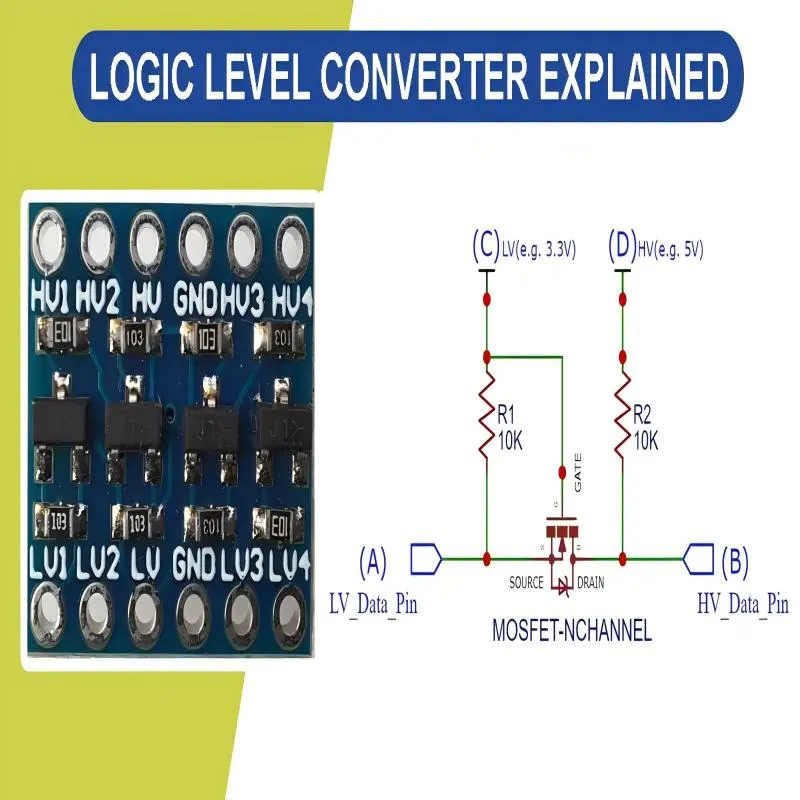
This figure is one of the technical core illustrations of the entire article. It expands and elaborates on the simplified circuit from Figure 3, providing complete circuit connections and labels. It serves as a “visual manual,” helping readers thoroughly understand the definition and function of each node in this classic topology, and is a prerequisite for understanding subsequent design tables (e.g., calculating pull-up resistors) and layout recommendations.
Place the level shifter where the voltage domains actually meet
This figure shifts the discussion from pure circuit theory to the critical PCB implementation. Through an abstract layout diagram, it visualizes one of the most common design mistakes (placing the converter arbitrarily) and its correct solution. This figure emphasizes that in mixed-voltage systems, physical layout is as important as electrical design, and extra trace length directly translates to loss of performance margin.
One mistake shows up again and again during board reviews: the level shifter is electrically correct, but physically misplaced. The MOSFET and pull-ups end up somewhere convenient for routing, not where the voltage domains actually cross.
On an I2C bus, that decision matters. Extra trace length is extra capacitance. Extra capacitance eats rise-time margin. Many “random” I2C problems are nothing more than a level shifter sitting five centimeters too far away from the MCU pins.
If this feels familiar, it’s because the same placement logic applies to other IO-sensitive parts. The reasoning is almost identical to how engineers approach transient protection placement, which is discussed in practical terms in the article on TVS diode selection and surge testing for IO protection.
Keep SDA and SCL boring
I2C does not reward creativity. Short traces. Matched lengths. No scenic routing tours across the board.
Avoid running SDA or SCL alongside switching nodes. If they must cross noisy areas, give them a solid ground reference underneath. In practice, a clean return path fixes more I2C problems than tweaking pull-up resistors ever will.
Ground matters more as voltages drop
Don’t ignore manufacturability
Small MOSFET packages solder just fine—until they don’t. Marginal joints here don’t always fail open. They fail intermittently. In production, that looks exactly like a communication bug.
Use known-good footprints. Give the pads room to wet. And don’t assume a tiny part is immune to assembly variation.
Validate your logic level shifter in the lab
Test it before the layout is “final”
It’s tempting to trust a reference design and move on. A quick breakout or test header can save weeks later. Being able to swap pull-up values and probe both sides of the bus is worth the extra afternoon.
This mirrors the workflow many teams already use when validating protection or interface circuits, a pattern that shows up repeatedly across practical hardware articles on tejte.com.
Use a scope, not just a logic analyzer
A logic analyzer will happily decode I2C frames that are already out of spec. A scope will not lie.
Look at rise time. Look at symmetry between SDA and SCL. Check behavior at the lowest supply voltage you expect to ship. If the waveform only looks “okay” under ideal conditions, it won’t stay okay.
Power sequencing reveals hidden problems
Mixed-voltage systems rarely power up cleanly. One rail comes up first. Another lags. Devices reset at different times.
Cycle power repeatedly. Watch what happens when one side of the level shifter is alive and the other isn’t. Many stuck-bus issues trace back to this phase, not steady-state operation.
Engineers who have dealt with polarity or sequencing problems before will recognize the pattern—it’s the same class of issue described in the reverse polarity protection circuit design guide, just showing up as a digital symptom instead of a burned component.
Turn lab results into a checklist
Follow industry trends in low-voltage MCUs and level shifters
IO voltages are not going back up
Every generation of low-power MCUs pushes IO levels lower. Power savings are real, but noise margin shrinks fast. Designs that were forgiving at 3.3 V become fragile at 1.8 V.
If your team already pays attention to IO stress and protection—topics that come up often in tejte.com’s semiconductor and interface guides—you’re already ahead of the curve.
Discrete solutions still matter, but margins are tighter
Designing for the next voltage, not just the current one
Solve common logic level shifter troubleshooting questions
It works at 100 kHz, but not at 400 kHz. Why?
Why does this circuit break SPI but works fine on I2C?
My bus sometimes stays low after reset.
Can I use the same design for 1.8 V, 3.3 V, and 5 V?
How do I know it’s safe for production?
Final note
Bonfon Office Building, Longgang District, Shenzhen City, Guangdong Province, China

A China-based OEM/ODM RF communications supplier
Table of Contents
Owning your OEM/ODM/Private Label for Electronic Devices andComponents is now easier than ever.
