Logic Level MOSFET Design for 3.3V and 5V Loads
Jan 5,2026
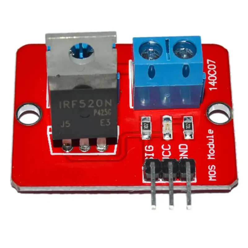
This is typically a simple MOSFET symbol or physical diagram placed below the article title, aiming to visualize the core theme of “logic-level MOSFET” and hint at its small yet critical role.
A logic level MOSFET almost never feels like a decision worth debating. It’s small, inexpensive, and familiar. In most designs, it gets dropped in late—after the MCU pinout is fixed and the power rails already feel “good enough.”
That’s exactly why it causes trouble.
On modern 3.3 V and 5 V boards, a single logic-level MOSFET often ends up doing far more than switching a trivial load. It gates sensor rails, isolates modules, drives LEDs under PWM, buffers fragile GPIO pins, and sometimes even sneaks into level-shifting roles. When the part is chosen by label alone, the failure mode is rarely dramatic. No sparks. No smoke. Just extra heat, unexplained voltage drop, or behavior that only becomes unstable once the product leaves the lab.
This article looks at logic level MOSFET design in real 3.3 V and 5 V systems, focusing on what actually happens at the gate rather than what the headline specs imply. We’ll connect switching theory with datasheet reality, show where logic-level behavior intersects with classic MOSFET as a switch design, and explain why some devices that look fine on paper quietly miss expectations in real hardware. If you already have a grounding in basic switching topologies from our earlier discussion of MOSFET switching practice in MOSFET as a Switch: Small-Signal Design Guide, think of this as the next layer down—where digital logic meets analog behavior.
How do logic level MOSFETs differ from standard MOSFETs?
Clarify what “logic level MOSFET” really means at 3.3 V and 5 V
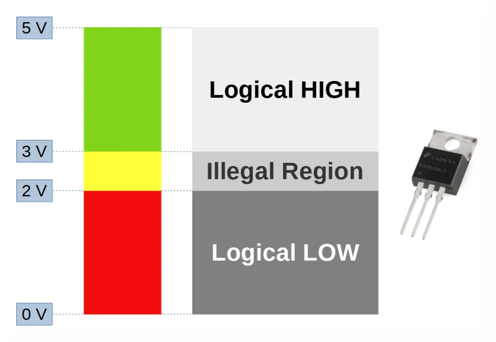
This is likely a chart with Gate-Source Voltage (Vgs) on the x-axis and Drain Current (Id) or conduction state on the y-axis. It clearly marks “Logical HIGH” (fully on), “Logical LOW” (off), and the “Illegal Region” in between which may lead to poor performance, emphasizing that Vgs(th) alone is insufficient for selection.
A logic level MOSFET is not defined by whether it turns on at some tiny gate voltage. That misunderstanding usually comes from over-reliance on Vgs(th). Threshold voltage only marks the point where the channel begins to conduct—often at a drain current so small it’s irrelevant for real switching.
What actually matters is simpler and stricter: can the MOSFET reach a low, well-specified Rds(on) at the gate voltage your logic can actually supply, typically 3.3 V or 5 V? If the answer is no, the device may technically turn on, but it will behave more like a lossy resistor than a clean switch.
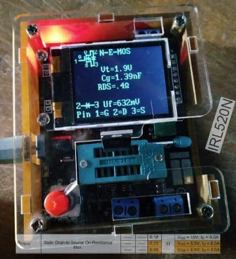
This distinction becomes critical on MCU-based boards. GPIO pins are expected to drive gates directly, without a dedicated driver stage. Many older power MOSFETs will tolerate that arrangement electrically, yet their Rds(on) at 3.3 V is high enough that dissipation rises quickly once current flows. The part “works,” but it never feels comfortable.
Compare logic level MOSFETs with small signal and power MOSFETs
A lot of confusion comes from mixing three related but distinct ideas.
Small signal MOSFETs are optimized for compact size and low gate charge. They typically live in SOT-23 or similar packages and handle modest currents. Some are excellent logic-level devices; others trade low Rds(on) for simplicity or cost. Being small does not automatically mean being logic-friendly.
Power MOSFETs, on the other hand, are built for current and thermal performance. Many legacy devices assume 8–10 V gate drive. Newer low-voltage trench parts often perform well at 4.5 V or even 2.5 V, but that behavior must be verified, not assumed.
A logic level MOSFET is defined neither by package nor by current rating. It’s defined by gate-drive behavior. A device can be a high-current power MOSFET and still qualify as logic-level—if its datasheet backs that up at low Vgs. This overlap is exactly where engineers get tripped up, especially when they assume “small signal” automatically means “safe for 3.3 V logic.” If that selection process feels familiar, the contrasts are explored in more detail in our Small Signal MOSFET Selection Guide.
Understand where MOSFET as a switch meets logic level behavior
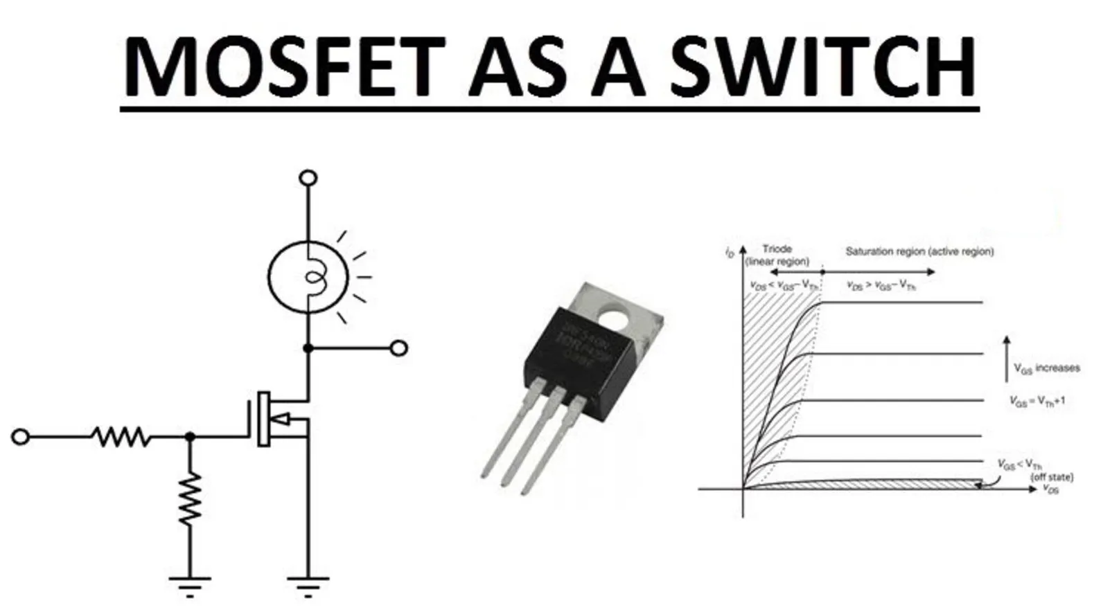
This figure might visually compare two different packages (e.g., SOT-23 vs. TO-220) or characteristic curves side-by-side to illustrate that “logic-level” is a category defined by gate-drive behavior, not package or current rating.
Most articles about mosfet as a switch focus on topology: low-side versus high-side switching, inductive loads, flyback paths, and protection components. All of that is essential, but it usually assumes one thing implicitly—that the gate can be driven properly.
Logic-level behavior answers a different question: can your digital logic drive this gate directly and still get predictable, cool switching? A MOSFET might work beautifully when driven by 10 V and perform poorly when driven by a 3.3 V GPIO. In that case, the switching concept is sound, but the logic interface is not.
This is why logic-level considerations aren’t optional on modern low-voltage MCU designs. They determine whether the switch you drew on the schematic behaves like a switch in the finished product.
How should you read logic level MOSFET datasheets at 3.3 V and 5 V?
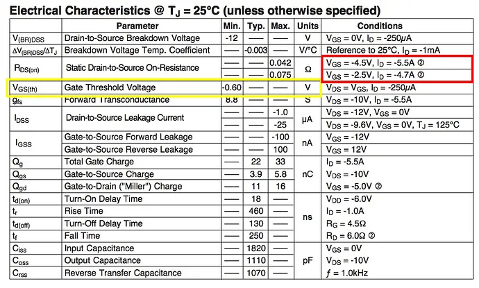
This is a screenshot of an actual MOSFET datasheet table, highlighting or including parameters like Rds(on) at Vgs = -2.5V and -4.5V, Vgs(th), and Qg. It serves as an example to guide engineers to focus on performance specified at actual logic voltages (e.g., 3.3V, 5V), not just at 10V drive.
Focus on Vgs(th), Rds(on) at logic voltages, and Id ratings
The first adjustment is mental: stop treating Vgs(th) as a design parameter. It’s useful for rough comparison, not for deciding whether a MOSFET will behave well at 3.3 V.
Instead, look for Rds(on) specified at 2.5 V, 4.5 V, or 5 V, along with transfer curves that show how drain current rises with gate voltage. Pay attention to whether those numbers are guaranteed limits or typical curves. A MOSFET that only specifies Rds(on) at 10 V is quietly signaling that low-voltage gate drive was not its primary design target.
The same caution applies to Id ratings. They are usually measured at high Vgs and under ideal thermal conditions. A device rated for several amps may still overheat when switching a much smaller load if it’s driven from 3.3 V and spends too much time in the linear region.
Check gate charge (Qg) and capacitances for logic speed limits
Even when Rds(on) looks acceptable, gate charge (Qg) can limit how practical a MOSFET is under direct logic control. MCU pins can only source and sink so much current. A device with large Qg will switch slowly, which increases switching loss and EMI once PWM frequencies rise.
At DC or very low switching rates, this often goes unnoticed. As soon as PWM creeps into the tens of kilohertz, the limitation becomes obvious. This same gate-charge bottleneck shows up when MOSFETs are used as discrete level shifters, which is why designs that rely on MOSFET-based translators for digital buses are usually constrained to slower protocols—a topic we cover in depth in the Logic Level Shifter Guide for I2C & MCU IO.
Verify maximum Vgs, body diode behavior, and safe operating area
One detail that catches engineers off guard is Vgs(max). Many logic-level MOSFETs are optimized for sensitivity, not brute-force gate robustness. It’s common to see absolute maximum ratings of ±10 V or ±12 V. That’s perfectly adequate for MCU-driven designs, but it leaves less margin for noise, ESD, or accidental overshoot.
This becomes relevant when:
- Gates are routed long distances
- Inductive loads inject fast transients
- External connectors expose the gate to ESD events
A logic-level device can survive electrically and still degrade if the gate oxide is stressed repeatedly. That’s why practical designs often include a small series gate resistor or localized protection rather than relying on the MOSFET alone.
The body diode also deserves attention. In low-voltage switching it often gets ignored, yet it defines how current flows during reverse or transient conditions. In motor drivers, relay outputs, or shared rails, the body diode can conduct unexpectedly and shift where dissipation occurs.
Finally, there’s the safe operating area (SOA). SOA curves tell you whether the MOSFET can survive operating in its linear region during turn-on, startup, or fault conditions. Logic-level MOSFETs driven at 3.3 V are more likely to linger in that linear region, especially when switching higher-voltage loads. If the SOA margin is thin, the device may run hot even when average current seems modest.
How can you use a logic level MOSFET to switch 3.3 V and 5 V loads safely?
Design low-side switches for LED strips, sensors, and modules
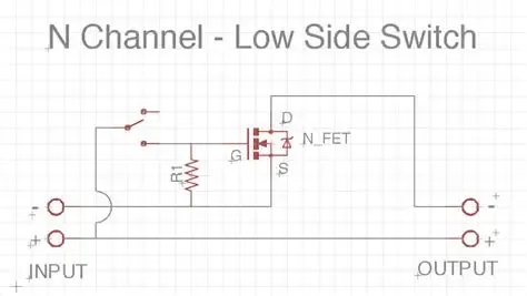
This is a simple circuit diagram containing an MCU GPIO, a resistor, an N-channel MOSFET, and a load to ground (e.g., an LED). It illustrates that the low-side switch is the most common and straightforward application for logic-level MOSFETs, with simple gate drive (Vgs = Vlogic).
The simplest and most forgiving configuration is still the low-side N-channel switch. With an n channel MOSFET transistor on the ground side, the gate-to-source voltage equals the logic output. There’s no ambiguity about headroom.
This topology works well for:
- LED strings and indicators
- Sensors and peripheral modules
- Low-power actuators
As long as the MOSFET’s Rds(on) is specified at your logic voltage, performance is predictable. Thermal behavior scales cleanly with current, and debugging is straightforward. If EMI or ringing appears, a modest gate resistor usually calms things down without side effects.
Many engineers learn switching fundamentals this way before moving on to more complex arrangements. If you’ve ever built a simple GPIO-controlled load and wondered why it behaved inconsistently at higher current, the root cause is often not the topology—but the assumption that “any MOSFET will do.”
Build high-side P-channel switches that respect gate headroom
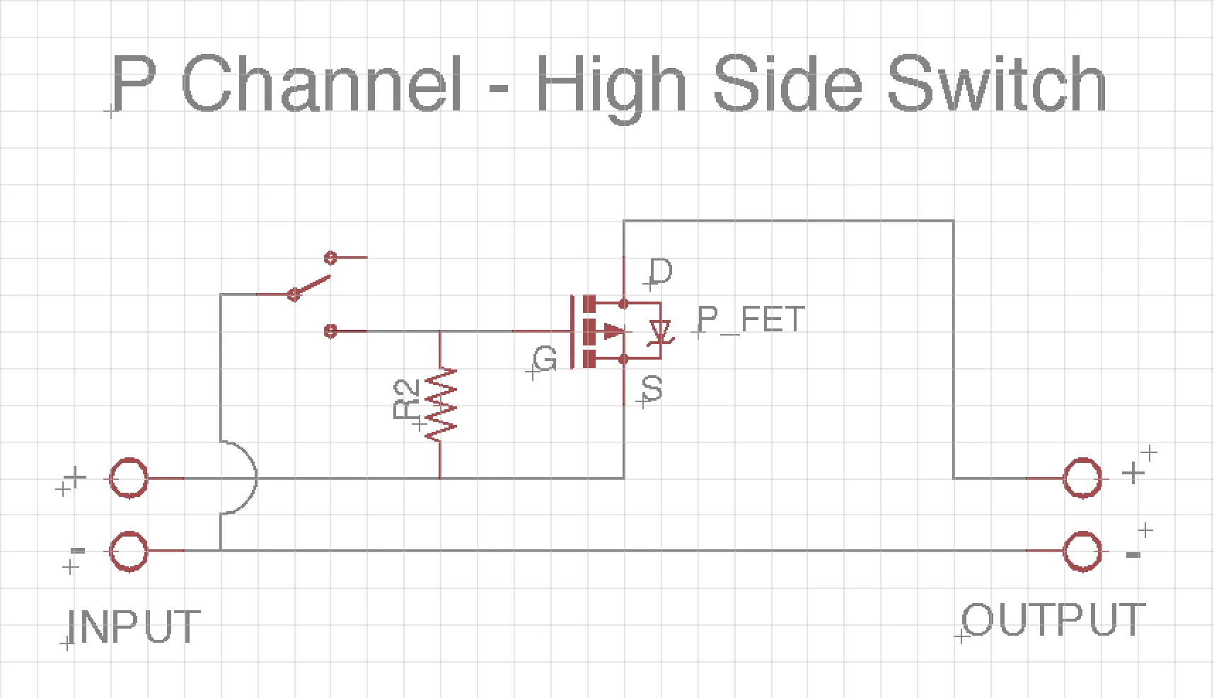
The schematic shows a P-channel MOSFET with its source connected to the supply, drain to the load, and the other side of the load to ground. The gate is controlled by an MCU via a resistor. This diagram is used to illustrate that when using a 3.3V logic signal to control a P-MOSFET on a 5V rail, the available Vgs is only -1.7V, which may be insufficient for full turn-on, leading to performance issues.
High-side switching looks attractive when you want the load referenced to ground, but logic-level constraints show up quickly. With a P-channel MOSFET on a 5 V rail and a 3.3 V control signal, the available Vgs is only −1.7 V. That’s rarely enough to reach low Rds(on).
Designers usually encounter this as:
- Unexpected voltage drop across the MOSFET
- Heat buildup at currents that “should be fine”
- Loads that behave normally at light current and sag under load
In these cases, the MOSFET may still qualify as “logic level” at 4.5 V, but not at the effective gate drive your circuit provides. This is where a level shifter or dedicated high-side switch becomes less of a luxury and more of a requirement.
Select logic level MOSFETs for 12 V loads driven by 3.3 V or 5 V
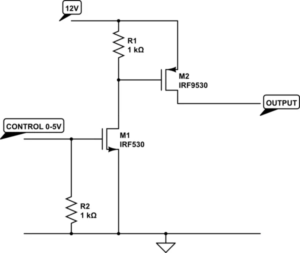
This schematic clearly depicts a circuit consisting of two MOSFETs (M1 N-channel, M2 P-channel) and two resistors. It solves the gate drive headroom issue for high-side P-MOSFETs mentioned in Figure 6, allowing low-voltage logic signals (e.g., 3.3V/5V) to efficiently switch higher voltage loads (e.g., 12V).
Switching a 12 V load from a 3.3 V or 5 V GPIO is possible, but expectations must change. At higher load voltage, the MOSFET spends more time dissipating energy during transitions. Rds(on) still matters, but SOA and thermal margin matter more.
In practice, the design question becomes: can the MOSFET survive worst-case conditions without relying on optimistic assumptions? That usually means checking conduction loss, transient stress, and package dissipation together. We’ve seen many otherwise solid designs fail here simply because logic-level behavior was assumed instead of verified—a scenario explored further in our discussion of 12 V switching limits for logic-driven devices in Logic Level MOSFETs in 12 V Load & SOA Design.
How do you check if your logic level MOSFET is really “logic-friendly”?
Define logic drive conditions for 1.8 V, 3.3 V, and 5 V systems
Each logic family sets a different bar. At 1.8 V, only a narrow set of MOSFETs behave well. At 3.3 V, many devices claim compatibility, but fewer deliver low loss. At 5 V, most logic-level parts finally operate in their comfort zone.
The goal isn’t “does it turn on?” but “does it switch cleanly, efficiently, and with thermal margin?”
Use a gate-drive and loss calculator to validate device choice
This is a structured table listing key input parameters (e.g., V_logic, I_load, Rds_on_spec) and core calculation formulas (conduction loss, voltage drop, thermal margin ratio). It serves as a practical tool to help engineers identify potential thermal or performance risks at the theoretical calculation stage, avoiding selection based solely on intuition.
| Parameter | Description |
|---|---|
| Vlogic V | GPIO or control voltage (1.8 / 3.3 / 5) |
| Vload V | Load supply voltage |
| Iload A | Load current (DC or RMS) |
| Rds_on_spec Ω | Datasheet Rds(on) at matching Vgs |
| Duty_cycle | PWM duty cycle (0-1; use 1 for static switching) |
| Ppackage_limit W | Allowed package dissipation |
Core calculations
• Conduction loss
P_cond_W = I_load_A² × Rds_on_spec_Ω × Duty_cycle
• Voltage drop
V_drop_V = I_load_A × Rds_on_spec_Ω
• Efficiency contribution
Eff_pct = (V_load_V − V_drop_V) / V_load_V × 100
• Thermal margin ratio
Thermal_margin_ratio = P_package_limit_W / P_cond_W
How to interpret the result
- ≥ 3 → comfortable margin
- 1.5–3 → check copper area or airflow
- < 1.5 → upgrade MOSFET or package
A final sanity check is the logic-compatibility flag. If the datasheet provides Rds(on) data near your actual gate voltage, the device earns a “yes.” If all performance data is tied to 10 V, treat it as a warning sign—even if marketing copy says otherwise.
Decide when you must add a dedicated MOSFET gate driver
A gate driver becomes necessary when:
- Gate charge overwhelms MCU pin drive
- PWM frequency rises
- Switching loss rivals conduction loss
In those cases, a small driver often costs less than the time spent chasing thermal or EMI issues later.
How can you use logic level MOSFETs inside level shifter circuits?
Review MOSFET-based bidirectional I²C level shifter topologies
The classic BSS138 level shifter circuit is a good example of how a logic-level MOSFET can act as a bidirectional level shifter rather than a hard switch. In this topology, the MOSFET is intentionally kept near its linear region. Pull-up resistors on both sides define logic levels, while the MOSFET and its body diode allow signals to propagate in either direction.
This approach works well because I²C is slow, open-drain, and tolerant of rise-time shaping. For these buses, a MOSFET-based I2C level shifter is simple, cheap, and robust. Many engineers first encounter logic-level behavior through this circuit, often without realizing how dependent it is on device characteristics like threshold voltage and capacitance.
Decide when to prefer a logic level converter IC over discrete MOSFETs
The simplicity of a MOSFET-based shifter can be misleading. As soon as edge rate, bandwidth, or bus loading becomes critical, its weaknesses show up. Rise times stretch. Signal integrity degrades. Margins shrink.
Integrated logic level converter ICs earn their place when:
- Multiple channels must switch together
- ESD protection matters
- Timing consistency is important
They remove ambiguity by design. That tradeoff—slightly higher BOM cost for predictability—is often worth it.
Choose between 3.3 V to 5 V level shifter options for SPI, UART, and GPIO
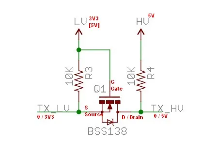
This schematic is the classic “BSS138” type level-shifter circuit, containing an N-channel MOSFET and pull-up resistors on both sides. It visually demonstrates the second common use of logic-level MOSFETs in digital interfaces—voltage translation—and implies its suitability for low-speed, open-drain buses.
A practical rule holds up well in the field:
MOSFET-based shifters are suitable for I²C, slow UART, and GPIO, but they are a poor fit for SPI or other high-speed buses. When engineers try to stretch a MOSFET level shifter beyond that comfort zone, failures tend to be intermittent and difficult to diagnose. If you’ve run into that situation before, the broader design context is discussed in more depth in our Logic Level Shifter Guide for I2C & MCU IO.
How do you lay out and protect logic level MOSFETs on mixed-voltage boards?
Place low-side and high-side devices with short, tight current loops
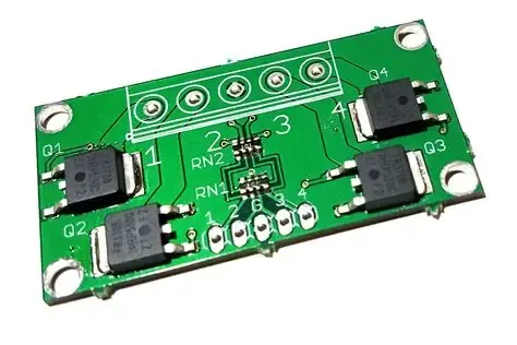
This is likely a top-view of a PCB layout, with highlighted lines or arrows indicating the current path from the supply, through the MOSFET, to the load, and back to ground. It emphasizes the critical role of compact and intentional layout on mixed-voltage boards to ensure stable operation of logic-level MOSFETs and prevent noise coupling.
Switching loops should be compact and intentional. Long gate traces act like antennas. Wide loops radiate EMI. Placing the MOSFET close to the load or connector shortens current paths and reduces unintended coupling.
This matters even more on mixed-voltage boards, where noisy load currents share space with sensitive logic.
Add flyback diodes, TVS, and snubbers for inductive loads
Inductive loads change the risk profile completely. Relays, motors, and solenoids will generate voltage spikes regardless of how “small” the MOSFET looks. A logic-level gate does not make the drain any less vulnerable.
A common protection stack includes:
- A flyback diode for basic energy recirculation
- A TVS diode for fast transients
- An RC snubber to control edge rate
Skipping these parts often works—until it doesn’t. If you’ve already dealt with unexplained MOSFET failures in inductive paths, the protection strategy is closely related to the approaches outlined in our article on flyback and transient suppression for MOSFET-switched loads at Flyback Diode Design for Relays and Motors.
Protect logic level gates from ESD and dV/dt stresses
How should you select drivers and pre-drivers for logic level MOSFETs?
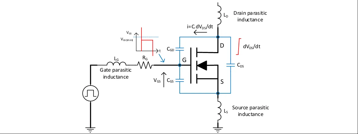
This diagram uses circuit model symbols (MOSFET, inductors) and waveforms to visualize how parasitic inductance in the loop (gate, drain, source) during turn-off of the low-side switch or load switching can cause harmful voltage spikes or oscillations, potentially turning on the MOSFET unexpectedly or damaging the gate oxide, thereby leading into the discussion of gate drivers.
Know when a MOSFET gate driver IC is worth adding
A driver earns its place when:
- Gate charge slows switching
- PWM frequency increases
- EMI or thermal margins tighten
In those cases, a driver doesn’t complicate the design—it stabilizes it.
Match driver output logic levels to 3.3 V and 5 V systems
Consider integrated driver + MOSFET solutions for compact designs
What recent trends are shaping logic level MOSFET and driver ICs?
Track how low and medium voltage MOSFET portfolios are evolving
Watch EV and SiC markets that still segment “logic level MOSFET”
Follow application notes on 3.3 V-compatible MOSFET selection
How do you avoid common mistakes with logic level MOSFETs in real products?
Why does a “logic level MOSFET” still overheat at 3.3 V gate drive?
Why won’t my 3.3 V MCU switch a 5 V or 12 V load cleanly?
When is a discrete level shifter the wrong tool for high-speed buses?
FAQ: Logic Level MOSFET Design Questions Engineers Actually Ask
How can I tell from a datasheet whether a MOSFET is truly logic level at 3.3 V?
Look for guaranteed Rds(on) data at or near 3.3 V. Threshold voltage alone is not enough.
Can a 3.3 V MCU safely drive a logic level MOSFET switching a 12 V load without a driver?
Sometimes, but only if conduction loss, SOA, and thermal margin all check out. Many designs underestimate this.
Is it safe to reuse the same logic level MOSFET design for both 3.3 V and 5 V boards?
Usually yes, but only if Vgs(max) and loss calculations remain within limits at both voltages.
When does a MOSFET-based level shifter stop being reliable?
As bus speed increases. I²C works well; high-speed SPI usually does not.
Why does my logic level MOSFET run hot even though current is far below its rating?
Ratings assume high gate drive and ideal cooling. Low Vgs and real PCB conditions change everything.
Should I choose a logic level MOSFET or a dedicated high-side switch IC for 3.3 V-controlled rails?
If protection, EMI, or certification matters, the IC often wins despite higher cost.
Closing perspective
Bonfon Office Building, Longgang District, Shenzhen City, Guangdong Province, China

A China-based OEM/ODM RF communications supplier
Table of Contents
Owning your OEM/ODM/Private Label for Electronic Devices andComponents is now easier than ever.
