ESD Protection for Microcontroller I/O
Jan 17,2026

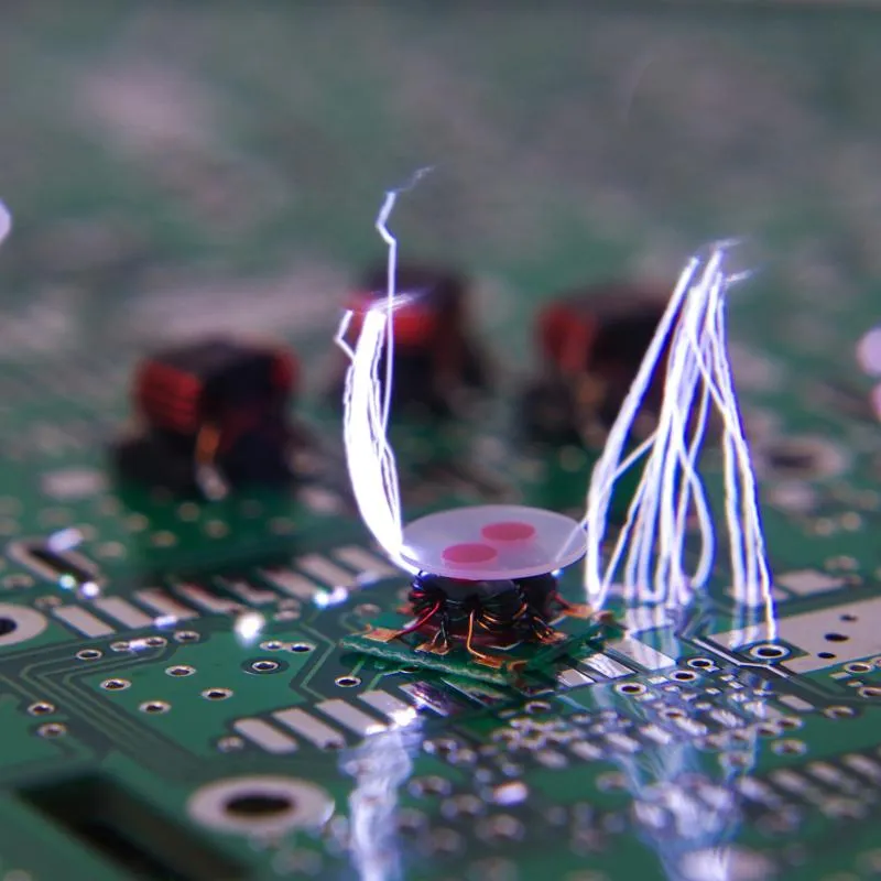
This image appears at the beginning to visually introduce the core challenge of ESD—its stealthy nature. It likely depicts a seemingly functional circuit board or device, but with visual cues (like tiny arcs, glitchy signal traces, or a question mark) hinting at internal instability caused by ESD, echoing the text: "A prototype boots normally... then suddenly there is a reset."
Electrostatic discharge rarely announces itself with a dramatic failure. Most of the time, it arrives quietly. A prototype boots normally on the bench, firmware runs without complaint, and basic tests pass. Then the board is installed in an enclosure, a cable gets longer, or someone plugs a connector during a dry winter morning. Suddenly, there is a reset. Or a communication error that disappears after a power cycle. That delayed, inconsistent behavior is where ESD protection around microcontroller I/O pins becomes relevant—and where it is most often underestimated.
This article focuses on board-level ESD protection for microcontroller I/O, not from a theoretical or compliance-only perspective, but from how ESD actually shows up in shipped products. The intent is to help you decide when protection is truly necessary, where ESD stress really flows on a PCB, and how to design protection that continues to work after the product leaves the lab.
Why should you plan ESD protection before microcontroller hardware design?
Understand how ESD failures really show up in MCU-based products
Titled “The Hidden Threat: ESD Damage in PCB Assembly,” this image is likely a close-up photo or diagram showing the actual physical damage an ESD event inflicts on a PCB or the internal structure of an MCU chip, such as tiny pits, fused interconnects, or damaged transistor gates. It visually explains why ESD leads to performance degradation like “peripherals that lock up once every few days” rather than complete failure.
Most ESD-related damage does not destroy a microcontroller outright. That is precisely why it is so easy to miss. Instead of a dead board, engineers see intermittent behavior: unexplained resets, peripherals that lock up once every few days, ADC readings that drift, or communication frames that fail sporadically. These failures are difficult to reproduce and even harder to debug because the system appears functional most of the time.
What usually happens is partial degradation. An ESD event stresses on-chip protection structures or thin oxide regions just enough to reduce margin, not enough to cause immediate failure. The MCU keeps running, but with less tolerance to noise, temperature, or voltage variation. Engineers who have dealt with field returns recognize this pattern quickly. ESD problems tend to surface after the hardware is considered “working,” which is exactly why planning protection early is more effective than trying to retrofit it later.
Align your ESD protection goals with IEC 61000-4-2 and OEM expectations

Explicitly titled “IEC 61000-4-2 Testing Lab,” this should be a photo depicting a real ESD testing scenario. It likely shows an ESD simulator (ESD gun) applying a contact or air discharge to the metal casing or interface of a device (e.g., a board with connectors or a finished product). A ground reference plane and test equipment might be in the background, emphasizing the difference between system-level and component-level testing.
At the system level, ESD immunity requirements almost always trace back to IEC 61000-4-2. This standard defines how ESD is applied to a product: contact discharge, air discharge, current waveform shape, and test levels such as ±4 kV, ±8 kV, or ±15 kV. Importantly, it is a system-level test, applied at connectors, exposed metal, and user-accessible points.
That distinction matters because many MCU datasheets list ESD ratings that apply only to the bare device under controlled conditions. Those ratings are primarily intended to guarantee survival during manufacturing, assembly, and basic handling. They do not imply that the assembled product will survive system-level ESD events applied through cables or connectors. Most OEM specifications reference IEC 61000-4-2 directly and expect the board designer to provide the necessary protection at the PCB level.
Decide which MCU boards actually justify external ESD protection
Not every design requires the same ESD strategy, and treating all boards identically often leads to either overdesign or unpleasant surprises. Consumer products with exposed connectors, buttons, or sensor ports usually justify external protection. Industrial control boards with long I/O cables almost always do. Automotive electronics typically require external ESD devices by default, even for relatively slow signals. Development and evaluation boards benefit from protection simply because they are handled, probed, and reconfigured frequently.
In contrast, tightly enclosed modules with only internal connections may only need reserved footprints for ESD components, populated later if testing or field experience demands it. The key is to make this decision intentionally during early design reviews. If ESD protection is never discussed at that stage, it almost always reappears later as a problem rather than a design choice.
How do ESD events actually stress MCU I/O pins and PCB structures?
Trace the real ESD current path through GPIO, ADC, and supply pins
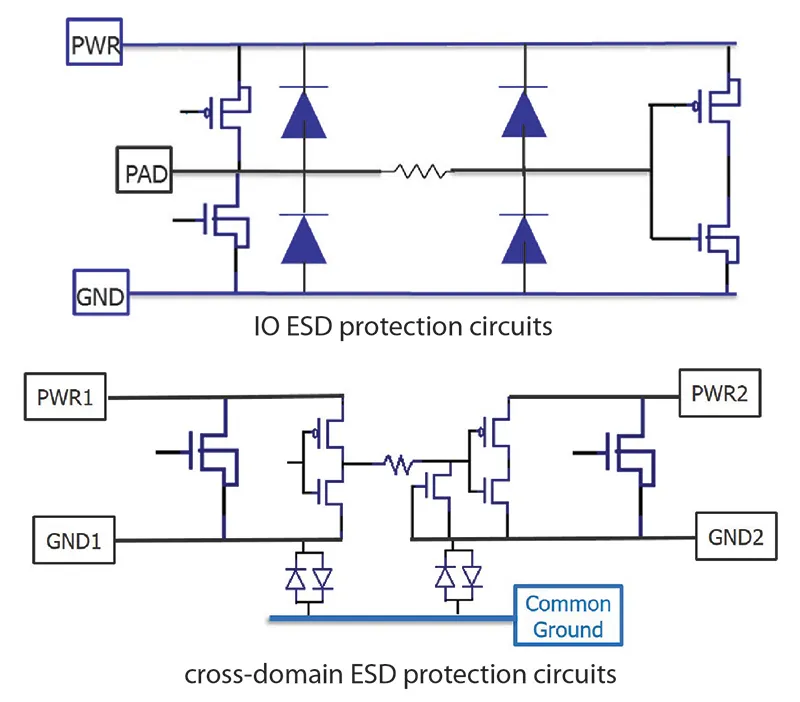
This image follows the subheading “Trace the real ESD current path through GPIO, ADC, and supply pins.” It is undoubtedly a schematic diagram visualizing how ESD current flows inside a microcontroller when an I/O pin is struck. Arrows likely show the current path: entering the pin, passing through internal parasitic or designed clamp diodes, moving to the VDD or VSS rails, and finally reaching the substrate and ground. This explains why internal protection structures can be overwhelmed.
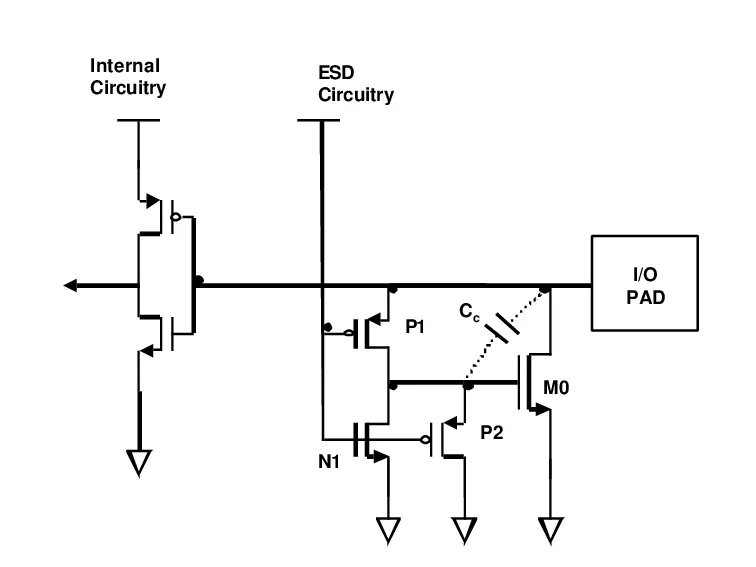
When an ESD event strikes an I/O pin, the current does not stop at the pad. It looks for the lowest-impedance path back to ground. In many MCU architectures, that path runs through internal clamp diodes into the silicon substrate and then into the power or ground network. Once ESD current enters the silicon, the risk of damage increases significantly.
Application notes from major MCU vendors consistently show that internal protection structures are small and optimized for limited stress. They are not designed to absorb repeated system-level ESD events. External ESD protection works because it intercepts the current before it reaches the MCU pin, redirecting it into a component designed to handle that energy.
Compare human body, contact discharge, and cable discharge events
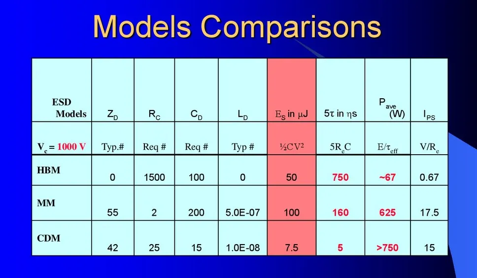
Based on the context, this image should include a comparison table (partially provided in the text) listing key parameters of different ESD models like Human Body Model (HBM), Machine Model (MM), and Charged Device Model (CDM), such as equivalent impedance, capacitance, discharge energy, and rise time. The image might graphically illustrate the differences in current waveforms or severity among these models, aiming to explain why a device rated for HBM can still fail IEC system-level testing.
A common source of confusion is treating all ESD models as equivalent. They are not. Human Body Model (HBM) ratings describe relatively slow, lower-current events used for device qualification. IEC 61000-4-2 contact and air discharge tests involve much faster edges and significantly higher peak currents. Cable discharge events can be even more severe, particularly when long harnesses store charge and release it suddenly.
This explains why a design that survives HBM ratings in a datasheet can still fail IEC testing at the system level. The stress mechanisms and current magnitudes are simply different.
Identify the most vulnerable entry points on your MCU board
This image precedes a paragraph discussing that certain board areas are more likely to experience ESD stress. It is likely a schematic or photo of a PCB, using arrows, highlighted areas, or labels to clearly indicate typical ESD entry points, such as USB ports, buttons, audio jacks, sensor terminals, and debug headers. This visually demonstrates why differentiated ESD protection is needed for different I/Os.
How should you choose between on-chip ESD robustness and external protection?
Interpret MCU datasheet ratings without over-trusting them
MCU datasheets often include ESD ratings, and those numbers are valid within their intended scope. They indicate that the device can survive manufacturing, assembly, and limited handling. They do not guarantee that the MCU can serve as the primary ESD protection element for a finished product subjected to system-level testing.
Relying solely on internal protection shifts all ESD stress into the MCU itself. When that approach fails, it usually fails expensively and unpredictably.
Decide when external ESD diodes are mandatory around MCU I/O
Separate power-rail TVS diodes from signal-line ESD diodes

Titled “A diagram showing how TVS diodes (ESD protection diodes) work,” this should be a classic circuit schematic showing an ESD/TVS diode connected between a signal line (to the MCU I/O) and ground. It might include a voltage waveform representing an ESD pulse and a flattened, safe waveform after clamping, visually comparing voltage levels with and without protection. The diode's off-state under normal voltage and rapid turn-on during overvoltage might also be indicated.
One frequent mistake is treating all TVS devices as interchangeable. Power rails such as 5 V, 12 V, or 24 V require higher-power TVS diodes designed to absorb surge energy. Signal lines, by contrast, need fast, low-capacitance ESD protection diodes that preserve signal integrity while clamping voltage quickly.
If you are already familiar with rail protection concepts from power-focused designs—such as those discussed in a TVS diode selection guide for power rails—it is important to recognize that MCU I/O protection follows a different set of constraints and trade-offs.
How do you select the right ESD protection diode and TVS device for MCU I/O?
Choosing an ESD device for microcontroller I/O is rarely about chasing the “best” datasheet number. In practice, it is about avoiding the wrong compromises. Many designs fail not because the ESD diode was too weak, but because it interacted poorly with the signal it was meant to protect.
Most MCU I/O problems linked to ESD come down to three things: clamping that happens too late, voltage that clamps too high, or capacitance that quietly distorts the signal long before any ESD event occurs. The challenge is balancing those factors without overengineering every pin.
Translate Vrwm, Vbr, Vclamp, and capacitance into real MCU limits
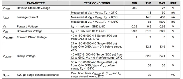
Titled “The definition of VRWM, VF, VBR, VFCCLAMP and VCLAMP in datasheet,” this is likely a characteristic curve or infographic visually explaining ESD diode datasheet parameters. It might show a typical diode V-I (Voltage-Current) curve with clear markers for key points like Reverse Stand-off Voltage, Breakdown Voltage, Forward Voltage, and Clamping Voltage at a specified pulse current, helping engineers translate abstract specs into practical design constraints.
Engineers often start by checking Vrwm, making sure it exceeds the normal signal voltage. That part is straightforward. Where things get murkier is Vclamp. This is the number that actually determines whether the MCU pin survives a fast ESD pulse, and it is also the one most likely to be misread.
Datasheets usually specify clamping voltage at a defined peak current under an IEC-style pulse. That value already assumes an ideal layout. In a real PCB, trace inductance and ground impedance add extra voltage on top. If the clamping voltage looks “just barely acceptable” on paper, it will almost certainly be too high in practice. Leaving margin is not conservative design—it is realistic design.
Capacitance deserves equal attention. For slow GPIO, extra capacitance often goes unnoticed. For faster interfaces, it can quietly degrade edge rates, timing margins, or EMI behavior. Many ESD issues blamed on firmware or noise are actually side effects of poorly chosen protection capacitance.
If you need a refresher on why ESD pulses behave this way, the electrostatic discharge overview explains why fast rise times make parasitics dominate real-world behavior.
Match device type to signal type instead of treating all I/O the same
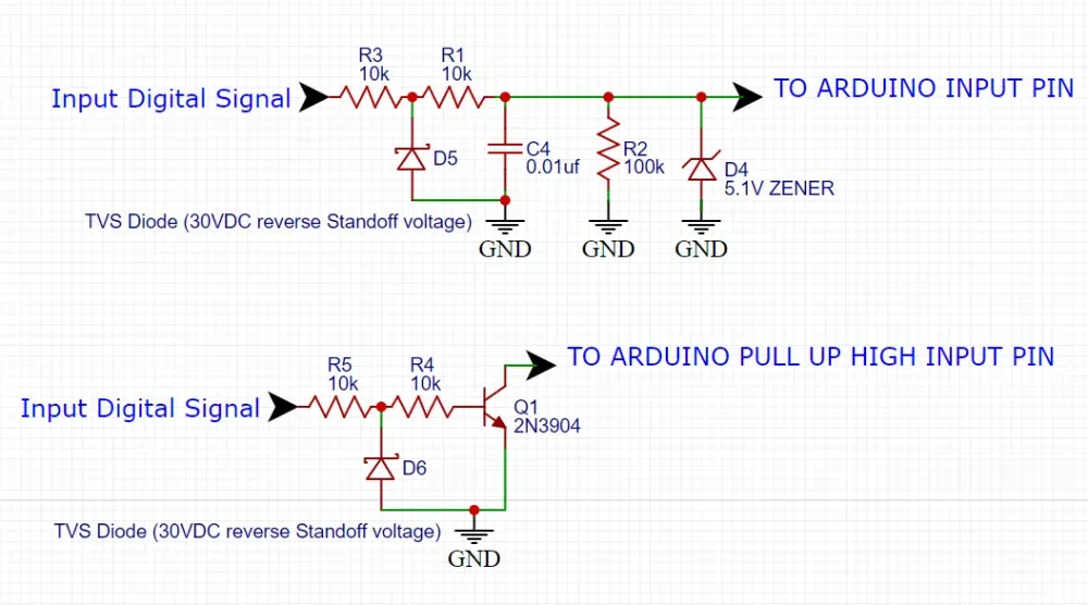
Titled “Esd Protection GPIO,” this should be a specific circuit schematic snippet showing how to configure external ESD protection for a typical General-Purpose Input/Output (GPIO) pin. It likely shows the GPIO pin connected to an external connector, with a series resistor (for current limiting) and an ESD protection diode (probably bi-directional) to ground placed along the path. This image is a concrete example of the advice to “match device type to signal type.”
One of the easiest mistakes to make is protecting every MCU pin with the same ESD part “for consistency.” That approach rarely survives first contact with real signals.
Slow GPIO lines and many ADC inputs tolerate higher capacitance and slower response. In fact, slightly larger junction capacitance can improve robustness by spreading the transient energy. UART, I²C, and SPI sit in the middle ground. They can accept some capacitance, but timing margins must be checked, especially across temperature.
High-speed or automotive interfaces such as CAN, LIN, or Ethernet are far less forgiving. These often require low-capacitance ESD arrays, even if that means accepting higher clamping voltage. At that point, layout quality matters more than the nominal datasheet numbers.
There is no universal ESD diode. If one part “works everywhere,” it is usually doing something poorly somewhere.
Use automotive-grade devices as reference points, not blindly as defaults
Automotive ESD diodes are useful because they are designed with harsh environments in mind. Devices like PESD1IVN27-AX are commonly used on in-vehicle networks where voltage transients, temperature extremes, and repeated ESD exposure are expected.
The value of these parts is not that they must be used everywhere, but that their datasheets are honest about stress conditions. Working voltage, pulse current, and clamping behavior are usually specified clearly. Even in non-automotive designs, these parameters make good reference points when deciding how much margin is reasonable for a given MCU I/O line.
Build an MCU I/O ESD protection selector matrix
Titled “I/O ESD Protection Circuitry” and located in the “Build an MCU I/O ESD protection selector matrix” section, this might be a composite image. The left side could show recommended ESD protection circuit topologies for several typical interfaces (e.g., UART, I²C, CAN), while the right side is linked to the “selector matrix” table mentioned in the text or presents a flowchart guiding engineers to choose a protection scheme based on signal type, data rate, environment, etc. This image aims to provide a quick reference and design aid.
To avoid re-litigating the same trade-offs on every project, many teams rely on a simple selector matrix. It does not replace engineering judgment, but it forces the right questions to be asked early.
MCU I/O ESD Protection Selector Matrix
| Input Parameter | Description |
|---|---|
| Signal type | GPIO, ADC, DAC, UART, I2C, SPI, CAN, LIN, Ethernet |
| Vio,max (V) | Maximum signal voltage including overshoot |
| Data rate / bandwidth | kHz, Mbps, or interface class |
| Line environment | Internal PCB, enclosure exit, cable, vehicle harness |
| Target ESD level | IEC 61000-4-2 ±4 kV / ±8 kV / ±15 kV |
| Allowed capacitance (pF) | From signal integrity or timing budget |
| MCU abs max (V) | Absolute maximum pin rating |
| Output | Guideline |
|---|---|
| Minimum Vrwm | Vrwm ≥ 1.1 × V io,max |
| Maximum Vclamp | Vclamp ≤ V_abs,max - safety margin |
| Safety margin | Typically 5-10% |
| Max diode capacitance | Depends on interface speed |
| Peak current class | Scaled to IEC target level |
| Package / array | Single-line or multi-line as routing allows |
| Qualification | Consumer, industrial, or AEC-Q101 |
How can you design robust ESD protection circuits around MCU I/O pins?
Start simple: series resistance and passive filtering
Before adding dedicated ESD devices everywhere, it is worth asking whether a small series resistor already solves most of the problem. Series resistance limits peak current and slows down fast transients. On low-frequency signals, that alone can dramatically reduce ESD stress.
Adding a small capacitor to ground forms a basic low-pass filter. This combination is often enough for configuration pins, buttons, and slow sensor inputs. The bandwidth penalty is real, but frequently far smaller than designers expect.
Use ESD diodes deliberately at external interfaces
Once a signal reaches an external connector, passive measures alone are rarely sufficient. Dedicated ESD protection diodes or arrays become necessary, not because the MCU is weak, but because the stress is uncontrolled.
The familiar topology—connector first, ESD diode to ground, then series resistance before the MCU—works because it keeps the highest current away from sensitive silicon. What determines success is not the symbol in the schematic, but the physical current loop. Long traces and indirect ground paths can defeat even the best ESD device.
This layout-first mindset aligns closely with system-level guidance in IEC 61000-4-2 immunity testing, where current paths and reference planes dominate outcomes more than component choice.
Treat mixed-signal and ADC inputs as part of the signal chain
For ADC inputs and precision references, ESD protection cannot be bolted on casually. Leakage current, temperature drift, and parasitic capacitance all matter. Aggressive clamping may protect against ESD but quietly degrade accuracy or stability.
In many precision designs, a modest resistor, careful filtering, and a low-leakage ESD diode provide better long-term behavior than a “stronger” clamp. Engineers who work regularly with mixed-signal boards tend to think of ESD protection as part of the analog front end, not as a separate feature.
How should you place and route ESD protection on dense PCBs?
If an ESD design fails in the field, it is rarely because the wrong diode was chosen. Much more often, the layout quietly undoes the protection long before the schematic ever gets a chance to help.
The first thing to accept is that ESD is a layout problem before it is a component problem. The discharge happens fast enough that copper geometry dominates behavior. At that time scale, every extra millimeter of trace matters more than most datasheet optimizations.
Place ESD devices where the discharge actually enters the board
An ESD diode only works if it sees the event early. That sounds obvious, but many boards place the diode close to the MCU because it feels “safer.” In reality, by the time the discharge reaches that location, the damage may already be done.
The diode belongs near the connector, not near the silicon. Electrically near, not visually near. A short trace, minimal vias, and a direct path to ground matter far more than clean symmetry or routing convenience. If the ESD current can reach the MCU pin before it reaches the diode, the protection is largely symbolic.
Give ESD current a clear way out
Clamping voltage is only half the story. Once the current is clamped, it still needs somewhere to go. If the return path is narrow, fragmented, or shared with sensitive circuitry, the voltage rise shows up in places you did not expect.
In practice, this is why dense boards often struggle with ESD. Ground planes are cut up. Return paths zigzag. The diode technically works, but the energy spreads across the board anyway. Multiple ground vias close to the ESD device and a continuous reference plane do more for ESD robustness than many component upgrades.
Watch for layout choices that cancel protection
Some layout patterns consistently cause trouble. Long stubs between the signal and the ESD diode slow the clamp response. Placing the diode behind a connector shield or filter network can isolate it just enough to miss the peak. Routing ESD-exposed traces alongside sensitive analog or high-speed lines invites coupling problems that only appear under stress.
None of these mistakes look dramatic in CAD. All of them show up during ESD testing.
How can you validate ESD protection performance before mass production?
Apply ESD in the same way users will
Formal compliance testing comes later. Early validation is about realism. Apply discharges where fingers go, where cables connect, and where metal is exposed. Do it with the enclosure installed if possible. A bare board that passes ESD testing can still fail once the product is assembled.
You do not need to start at the maximum voltage. Lower levels already reveal weak points. A short overview of how these system-level tests are structured is available in the IEC 61000-4-2 overview, but the key lesson is simple: the stress is applied to the product, not the component.
Look for soft failures, not just survival
A board that “does not die” is not necessarily acceptable. Resets, dropped packets, ADC glitches, or brief lockups all indicate that ESD energy is still reaching sensitive circuitry. These soft failures are often precursors to long-term reliability problems.
Good teams log behavior, not just outcomes. They note which interface misbehaves, under what polarity, and at what stress level. That information almost always points back to a specific routing or grounding issue.
Write things down, even if it feels tedious
ESD test results tend to live in notebooks, photos, and half-remembered conversations. That is a mistake. Simple documentation—where discharges were applied, what happened, what changed—turns painful testing into reusable knowledge.
Months later, when the same MCU or interface appears in a new project, those notes prevent repeating the same mistakes.
What are the latest trends in ESD protection for MCU and automotive systems?
Higher data rates push capacitance lower
The move toward higher operating voltages, including 48 V domains in automotive and industrial systems, has expanded the range of ESD devices. Protection parts now need to tolerate higher steady-state voltages without becoming electrically intrusive during normal operation.
This has blurred the line between traditional signal-line ESD devices and higher-voltage transient suppressors, especially on mixed-voltage boards.
FAQ
The MCU claims IEC ESD robustness. Isn’t that enough?
Usually not. Those ratings help the chip survive handling and basic stress. They do not guarantee system-level immunity at connectors or cables. External protection shifts risk away from the MCU.
How close is ‘close enough’ for an ESD diode?
Close enough that the discharge sees the diode before it sees the MCU. In practice, that means a few millimeters and a clean ground return.
Can one protection device cover multiple GPIOs?
Only if it is designed for that purpose and routed correctly. Sharing a single clamp across scattered pins usually leaves some of them exposed.
What about ADC inputs?
They need protection, but not at the expense of accuracy. Modest resistance, gentle filtering, and low-leakage clamps usually work better than aggressive solutions.
How do I know if clamping is safe for the MCU?
If the worst-case clamping voltage is close to the MCU’s absolute maximum, it is not safe. Layout and tolerance will push it higher in reality.
How do we test without destroying prototypes?
Start low, observe behavior, and increase stress gradually. Most useful insights appear well before maximum voltage is reached.
Bonfon Office Building, Longgang District, Shenzhen City, Guangdong Province, China

A China-based OEM/ODM RF communications supplier
Table of Contents
Owning your OEM/ODM/Private Label for Electronic Devices andComponents is now easier than ever.
