ESD Protection Diode Guide (PESD5V0S1BAF)
Nov 13,2025
Decide When a General-Purpose ESD Protection Diode Fits 5 V Rails

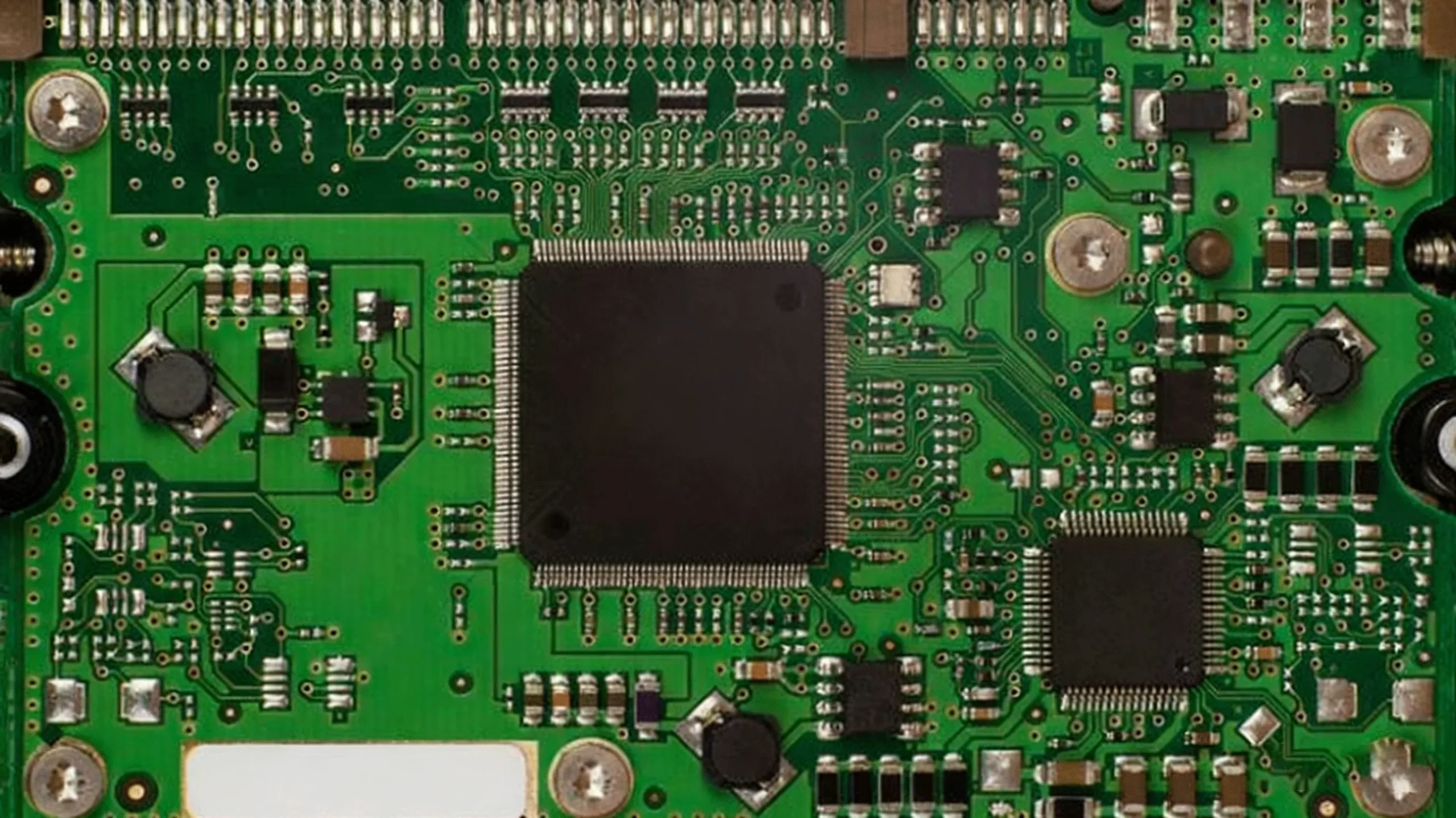
The photo illustrates a bench ESD test on a 5 V MCU board. The PESD5V0S1BAF is mounted next to the connector and tied to ground with two adjacent vias, minimizing loop inductance during IEC 61000-4-2 contact discharges.
Every engineer who’s wrestled with board-level ESD knows the dance between simplicity and performance. You could choose a specialized low-capacitance array, or you could reach for a solid 5 V general-purpose ESD diode that simply clamps and survives. The PESD5V0S1BAF sits squarely in that second camp—robust, compact, and tuned for the kind of 5 V domains that populate most embedded systems.
In typical 5 V logic, you’ll find several node types:
- Power rails feeding logic and sensors
- GPIO pins toggling LEDs or relays
- Push-button interfaces where a finger can easily inject a ±8 kV strike
- UART or I²C lines that are low-speed but sensitive to overshoot
For all of these, a small SOD-323 package like the PESD5V0S1BAF offers reliable clamping without the complexity of multi-channel arrays. Its bidirectional Zener construction keeps it symmetrical, so you don’t need to worry about signal polarity reversal during test or misconnection.
When you’re mapping node requirements, remember this practical rule:
If your signal bandwidth is under 10 MHz and capacitance up to 35 pF is acceptable, a general-purpose diode will often outperform “ultra-low-C” parts in real energy absorption. At 30–50 pF, you get a wider junction area and lower dynamic resistance—useful when the board ground isn’t ideal.
Before dropping any ESD device into the design, cross-check its role. Rail protection is not the same as data-line protection:
- Rail lines tolerate higher capacitance and slower recovery; you’re clamping bulk energy.
- Data lines, especially high-speed or RF ones, need low-C parts or π-filters to avoid signal distortion.
At TEJTE, we often place this diode near the connector on test jigs and MCU boards, tied to a solid ground via two adjacent vias—a simple practice that makes the difference between “no upset” and “mysterious resets.”
(You can learn more about related TVS diode selection practices in our TVS Diode Selection & Testing Guide on tejte.com.)
How Should You Set Clamping Voltage Targets for 5 V GPIO?
If you’ve ever scoped an IEC 61000-4-2 strike, you know the waveform isn’t gentle. A few nanoseconds after contact, the voltage can spike far above 8 kV—and what matters most is how high your GPIO pin rises before the ESD diode bites. That’s the clamping voltage (V C )—and getting it right separates a robust design from a fragile one.
For a 5 V GPIO, your safe headroom should keep V CL(max) below the absolute maximum rating of the pin (often 6 V–7 V for MCUs). The PESD5V0S1BAF, with a maximum clamping voltage of 14 V at 12 A (8/20 µs), sounds high, but remember: that figure reflects surge energy, not the microsecond-scale ESD event. In practice, its dynamic resistance limits the transient overshoot, keeping the protected node within survival range.
Here’s what to look for in datasheets:
| Parameter | Symbol | Typical Value | Interpretation |
|---|---|---|---|
| Reverse working voltage | VRWM | 5 V | Continuous safe voltage |
| Breakdown voltage | VBR (min) | 5.5 V | Trigger starts here |
| Clamping voltage | VC (max) | 14 V @ IPP = 12 A | Upper bound under strike |
| Peak pulse current | IPP | 12 A (8/20 μs) | Withstand strength |
| Peak pulse power | PPPPM | 130 W | Energy tolerance |
| Junction capacitance | Cd | 35 pF @ 1 MHz | Signal impact |
| Package | — | SOD-323 | Compact SMD footprint |
Rather than fixate on any single number, read V RWM , V BR , and V C together. They form a three-point curve—continuous bias, trigger, and clamp. A good practice is to select parts with V RWM ≈ system voltage, V BR just above nominal, and V C safely below IC limits.
Don’t forget parasitics. A 10 mm trace from the diode to ground can add several nanohenries of inductance, which easily turns into volts of overshoot. The shortest, fattest path is always the best one.
We’ve measured in real boards that a tight ground loop (two vias ≤ 2 mm apart) can reduce peak clamp by 20–25 %. That’s often the margin that decides whether a board passes its first IEC 61000-4-2 qualification.
If you’re working on mixed-signal power rails, see also our article on surge/TVS on power rails for pairing transient suppressors with MOSFET gate protection strategies.
Choose Bidirectional vs Unidirectional for Mixed-Polarity Nodes

The diagram maps where to place PESD5V0S1BAF on common 5 V nodes—rails, GPIOs, buttons, and UART. Positioning diodes at the connector with a short, direct ground return improves clamp effectiveness and reduces upset.
Polarity can be deceiving in real systems. Some GPIOs idle low but swing above 0 V due to AC coupling, while sensor lines may see reverse transients during hot-plug events. That’s why choosing between bidirectional and unidirectional ESD diodes isn’t as trivial as it sounds.
- Bidirectional diodes like the PESD5V0S1BAF behave symmetrically, clamping both positive and negative surges. They’re ideal for AC-coupled, differential, or undefined-polarity signals (e.g., UART RX/TX on floating grounds).
- Unidirectional diodes act more like standard TVS devices—they have a forward drop (~0.7 V) and a reverse breakdown region. They offer slightly lower forward conduction voltage, making them good for DC-biased lines where polarity is fixed.
For 5 V logic lines that occasionally experience negative swing or float during power-down, bidirectional is the safer default. It prevents reverse bias conduction that could unintentionally leak current into the IC’s substrate.
Still, there’s nuance. If you’re protecting a regulated 5 V supply rail, a unidirectional TVS diode with lower forward voltage can give faster clamping. On the other hand, for mixed-polarity GPIOs or buttons, you’ll appreciate the resilience of a bidirectional Zener like the PESD5V0S1BAF.
A few trade-offs to keep in mind:
- Capacitance: bidirectional ≈ double the junction area → higher C d , but stronger clamp.
- Reverse leakage: typically < 1 µA at 3.3–5 V, negligible in most control lines.
- Temperature stability: automotive-grade AEC-Q100 parts maintain spec up to 150 °C junction—a real edge for under-hood electronics.
Many engineers we’ve worked with found that swapping to a bidirectional SOD-323 part solved unexplained resets in button-rich control panels. The fix wasn’t magic—just symmetry.
If your design includes both kinds of nodes, don’t reuse the same footprint blindly. Assign separate symbols for uni- and bidirectional variants in your schematic library to avoid mix-ups during layout.
For high-speed differential or AC-coupled interfaces, stay tuned for our upcoming ESD layout guide on IEC 61000-4-2 layout practices, where we’ll show scope-verified examples of real strike paths and ground stitching effects.
Follow PCB ESD Layout That Actually Clamps
Many engineers trust the datasheet too much and forget the board decides whether an ESD protection diode ever reaches its advertised clamping voltage. A diode can only protect what it “sees” electrically—if your layout adds stray inductance, the strike will jump elsewhere long before the junction reacts.
A few layout rules separate a passing board from one that mysteriously resets under the IEC 61000-4-2 gun:
- Place the diode as close as possible to the connector.
The current path must be the shortest route to ground—every extra millimeter adds voltage overshoot. In practice, keep trace length < 5 mm between pin and pad.
- Use a fat, direct return to ground.
Ideally, a via stitched right beside the pad. Two vias spaced ≤ 2 mm apart can drop inductive voltage by 20–30 %.
- Avoid long stubs.
Once the protected trace passes the ESD device, never route back toward the connector; reflections there turn into secondary pulses.
- Keep protected traces behind the diode.
The protection point should be at the interface, not halfway inside the PCB.
During IEC 61000-4-2 qualification, engineers sometimes probe at the wrong point. The correct place to measure is between the protected node and the device ground return—not at the IC pin. A clean clamp waveform and “no upset” after multiple 8 kV contact strikes are what matter, not an arbitrary voltage number.
At TEJTE, we routinely validate layouts on small MCU boards and share results in our IEC 61000-4-2 layout practices article—showing how a 2-via return can outperform thicker traces without good stitching. This kind of grounding discipline matters more than any datasheet curve.
Verify Parts Against IEC Without Overdesigning
It’s tempting to pick the biggest, toughest TVS diode in the catalog, but oversizing can backfire. Devices built for high surge energy often have higher capacitance and slower response. The key is matching the protection level to the ESD environment—not designing for lightning when you’re defending against fingertip discharges.
The IEC 61000-4-2 waveform differs from the 8/20 µs pulse found in vendor datasheets.
Vendors like Nexperia, Littelfuse, and Vishay specify I PP (8/20 µs) mainly for surge power rating, but real ESD events are shorter (~0.7 ns rise). That’s where dynamic resistance (R dyn ) matters more than sheer current.
When interpreting curves:
- The 8/20 µs I PP tells you long-term energy capability.
- The IEC strike curve shows how fast the diode clamps.
- R dyn ≈ (V C − V BR )/I peak gives a quick field-level estimate of actual slope.
For the PESD5V0S1BAF, the math works out roughly as:
V BR = 5.5 V, V C = 14 V @ 12 A → R dyn ≈ 0.7 Ω.
That’s tight for a SOD-323 automotive-grade diode, meaning voltage rise under IEC pulse stays within safe GPIO limits when routing is short.
Let’s restate its verified parameters:
- VRWM = 5 V, VBR ≥ 5.5 V, VC ≤ 14 V @ 12 A (8/20 µs)
- PPPM = 130 W, C d ≈ 35 pF @ 1 MHz
- TJ max = 150 °C, AEC-Q100 qualified
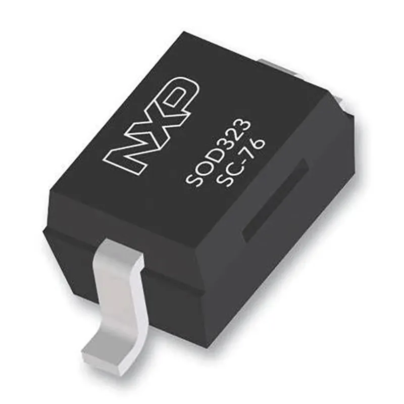
- Package = SOD-323 (SC-76), MSL 1, RoHS 3 / REACH compliant
In other words, you’re getting a diode that can take serious energy without loading down slow 5 V lines. Over-spec parts—say 1 kW SMA TVS—add 200 pF and 20 mm² of pad area for no gain on GPIOs.
That’s why, in TEJTE’s lab guidelines, we pair compact SOD-323 devices for local ESD defense and reserve high-power SMA TVS only for DC jack and 24 V rails.
If you’d like deeper testing workflows, our TVS Diode Selection & Testing Guide expands on pass/fail criteria and waveform validation—useful when you’re planning pre-compliance.
Apply PESD5V0S1BAF on Common Nodes (GPIO, UART/I²C, Buttons)
1. GPIO and Button Lines
These are classic slow ESD targets—often connected to metal buttons or cable shields.
A 35 pF junction barely affects <10 kHz inputs but gives strong current handling.
Place the diode right behind the connector or button pad, and tie its ground to a star-routed return or chassis via a short trace. In practice, two vias and a 2 mm loop keep voltage spikes under 10 V even at 8 kV contact strikes.
2. UART / I²C / Low-Speed Sensors
Serial interfaces that idle high benefit from the bidirectional 5 V rail protection this part offers.
At ≤ 400 kHz I²C speeds, the 35 pF capacitance translates to ~0.01 dB loss—negligible.
It’s why we routinely select this part on sensor boards used for environmental data or control modules.
If you’re protecting faster buses (USB 2.0 or HDMI), the same PESD family offers ultra-low-C variants. See our related post Coaxial Cable to HDMI Adapter Guide for a look at high-frequency signal considerations.
3. Production Notes and Handling

The chart visualizes datasheet parameters: VRWM≈5 V, VBR≥5.5 V, and VC≈14 V at 12 A (8/20 μs). With ~0.7 Ω dynamic resistance, the device limits overshoot during IEC 61000-4-2 events if the ground path remains very short.
The SOD-323 package handles automated assembly easily—compatible with both tape-and-reel and cut-tape packaging.
With MSL 1, there’s no special dry-pack requirement.
Its AEC-Q100 qualification and 150 °C junction rating make it safe for automotive or industrial boards.
During inspection, always confirm orientation (the laser mark denotes cathode) even for bidirectional parts; misplacement won’t kill the diode but can alter solder fillet size.
In TEJTE’s manufacturing runs, we use Digi-Reel feed for small-batch validation, then switch to full TR spools for volume SMT—ensuring consistent pick-and-place alignment.
If your design integrates both surge and hot-plug events, combine this diode with entry-point limiting devices as discussed in our hot-plug and rail hardening article. Together they form a holistic protection chain—from connector tip to silicon core.
Track 2025 Updates That Should Influence Your BOM
Component choices never stay static. If you’re designing for a 3- to 5-year product lifetime, the ESD protection landscape you use today may not look the same next revision cycle. By 2025, several vendors have begun pushing into new territory—higher bandwidth, lower clamp, and smaller packages.
Nexperia recently announced 48 V automotive communication ESD diodes aimed at CAN FD, LIN, and FlexRay lines on higher board voltages. These expand on the same PESD family used in 5 V systems like the PESD5V0S1BAF, but extend standoff voltage and current-pulse width for heavy automotive domains. Designers who once used two discrete 5 V diodes may soon replace them with a single 48 V variant per node.
At the opposite end, USB4 / Thunderbolt channels are demanding < 0.3 pF protection. Nexperia’s and Littelfuse’s new lines demonstrate how ultra-low-capacitance ESD diodes trade power handling for cleaner signal edges above 10 GHz. If your board mixes low-speed GPIO with high-speed links, segment your BOM early: the 35 pF SOD-323 part belongs to logic and sensor rails, not the differential pairs.
Meanwhile, Vishay and Littelfuse have both introduced fold-back TVS architectures that clamp lower at low current and then self-recover, letting automotive designs survive repeated 8 kV hits without thermal drift. For future-proofing, consider adding a “review trigger” in your internal database—if the next generation of your product targets 48 V rails or USB4 interfaces, it’s time to re-evaluate your ESD diode family.
The goal isn’t chasing the newest part—it’s knowing when performance ceilings or capacitance floors actually change your system-level reliability.
5 V Clamp Quick Picker & Pass Criteria
| Input Field | Example Entry | Check Logic / Criterion | Accept Range or Result |
|---|---|---|---|
| Node Type | 5 V Rail / GPIO (Slow) / UART-I²C | Defines cap threshold and clamp limit | — |
| V_abs_max_pin | 6.0 V (MCU limit) | For margin check | ≥ V_CL + 0.5 V |
| Target ESD Level | 8 kV contact | Chooses test severity | 4 kV / 8 kV |
| Candidate (VRWM, VBR, VC@IPP, Cd) | 5 V, 5.5 V, 14 V, 35 pF | Datasheet input | — |
| Clamp Margin | V_abs_max – VC ≈ −8 V (overshoot risk) | Must be > 0 | > 0 → Pass |
| Cap OK? | 35 pF for GPIO Slow | GPIO ≤ 50 pF, UART ≤ 30 pF | OK |
| Layout Score (0-3) | Connector placement = 1; short loop = 1; dual via = 1 | ≥ 2 = acceptable | 3 → Excellent |
| Result | "Go" if all conditions pass else "Review" | else “Review” | Go / Review |
In field validation, TEJTE engineers run this quick check before ordering new ESD parts. It ensures three things:
- Electrical headroom > 0 V margin (no over-clamp).
- Capacitance stays within functional limits.
- Layout implementation isn’t neglected.
The simple formula V_CL ≈ V_BR + I_peak × R_dyn helps approximate worst-case clamp. With R_dyn ≈ 0.7 Ω for PESD5V0S1BAF, a 12 A spike adds 8.4 V to the 5.5 V breakdown, roughly 13.9 V—matching the datasheet value and confirming model integrity.
This quick-picker table can later evolve into a calculator block on your WordPress post, similar to the selection matrices used in TEJTE’s RF Connector Selection Guides. It turns a static blog into a decision tool—something search engines and engineers both value.
FAQs – Common Questions About ESD Protection and PESD5V0S1BAF
Q1. What kind of diode is best for ESD protection on 5 V GPIO?
Use a bidirectional ESD protection diode with VRWM ≈ 5 V and low clamping voltage at the IEC level you’ll test. For slow GPIO or buttons, 30–50 pF is usually fine. Mount it at the connector and tie it to a wide ground via for short return.
Q2. How much current capability should a TVS have to pass IEC 61000-4-2?
The IEC test pulse is faster than an 8/20 µs surge, so published I PP values are only guides. Choose a part explicitly rated for IEC 61000-4-2, check its VC at 8 kV contact, and minimize loop inductance. A well-routed PESD5V0S1BAF easily handles 12 A (8/20 µs) with ≈14 V clamp.
Q3. What is an ESD protection diode and how does it differ from a surge TVS?
An ESD diode is a miniaturized, fast-reacting TVS diode optimized for short, low-energy spikes (< 1 µs). A surge TVS handles longer pulses (EFT or ISO 7637) and usually has higher capacitance. Match the part to the threat and bandwidth—see our TVS Diode Selection Matrix for details.
Q4. When should I choose bidirectional over unidirectional ESD diodes?
Whenever signal polarity may reverse or AC-couple—UART, sensor inputs, or plug-detect pins—go bidirectional. For strictly DC-biased power rails, unidirectional diodes can offer lower forward drop and slightly faster trigger.
Q5. Can I reuse one ESD part for both 5 V rails and high-speed USB4?
Rarely. USB4 and Thunderbolt operate at > 10 GHz and require < 1 pF capacitance. General-purpose SOD-323 ESD diodes like the PESD5V0S1BAF belong on logic and sensor lines, not RF or super-speed links. Use families built for ultra-low-C protection instead.
Q6. What’s a practical pass criterion for a board-level ESD test?
A board passes if there’s no latch-up, no functional upset, and signals return within tolerance after repeated strikes at the specified contact / air levels. On a scope, you should see a clean clamp near the diode and no damage to the IC. That’s exactly how we verify production runs at TEJTE’s test bench.
Q7. Why does my board still fail ESD tests even with an ESD diode?
Often, the diode is placed too far from the connector or tied to a floating ground island. The fix isn’t another part—it’s layout discipline. Keep the loop short, ground solid, and verify with oscilloscope strikes.
Final Notes

The side-by-side illustration compares correct placement (ESD diode next to connector, two vias within ~2 mm) versus a poor layout with long stubs. The former reduces inductive overshoot and improves pass rates in IEC tests.
The PESD5V0S1BAF remains a well-balanced ESD protection diode—robust, compact, and automotive-qualified. Its combination of 5 V standoff, 14 V clamp, 12 A pulse rating, and 35 pF capacitance makes it a sweet spot for 5 V logic, sensor, and control interfaces. When paired with careful layout and sensible testing, it offers the right balance between speed and survivability—an engineer’s friend in a world full of static.
For further reading on power-path hardening and transient control, check TEJTE’s related articles such as Logic-Level MOSFET in 12 V Design and Inrush Current Limiter with NCP45560.
Bonfon Office Building, Longgang District, Shenzhen City, Guangdong Province, China

A China-based OEM/ODM RF communications supplier
Table of Contents
Owning your OEM/ODM/Private Label for Electronic Devices andComponents is now easier than ever.
