SMP RF Connector Design for Board-to-Board and Cable Systems
Feb 06,2026
Map where an SMP RF connector actually belongs in your system

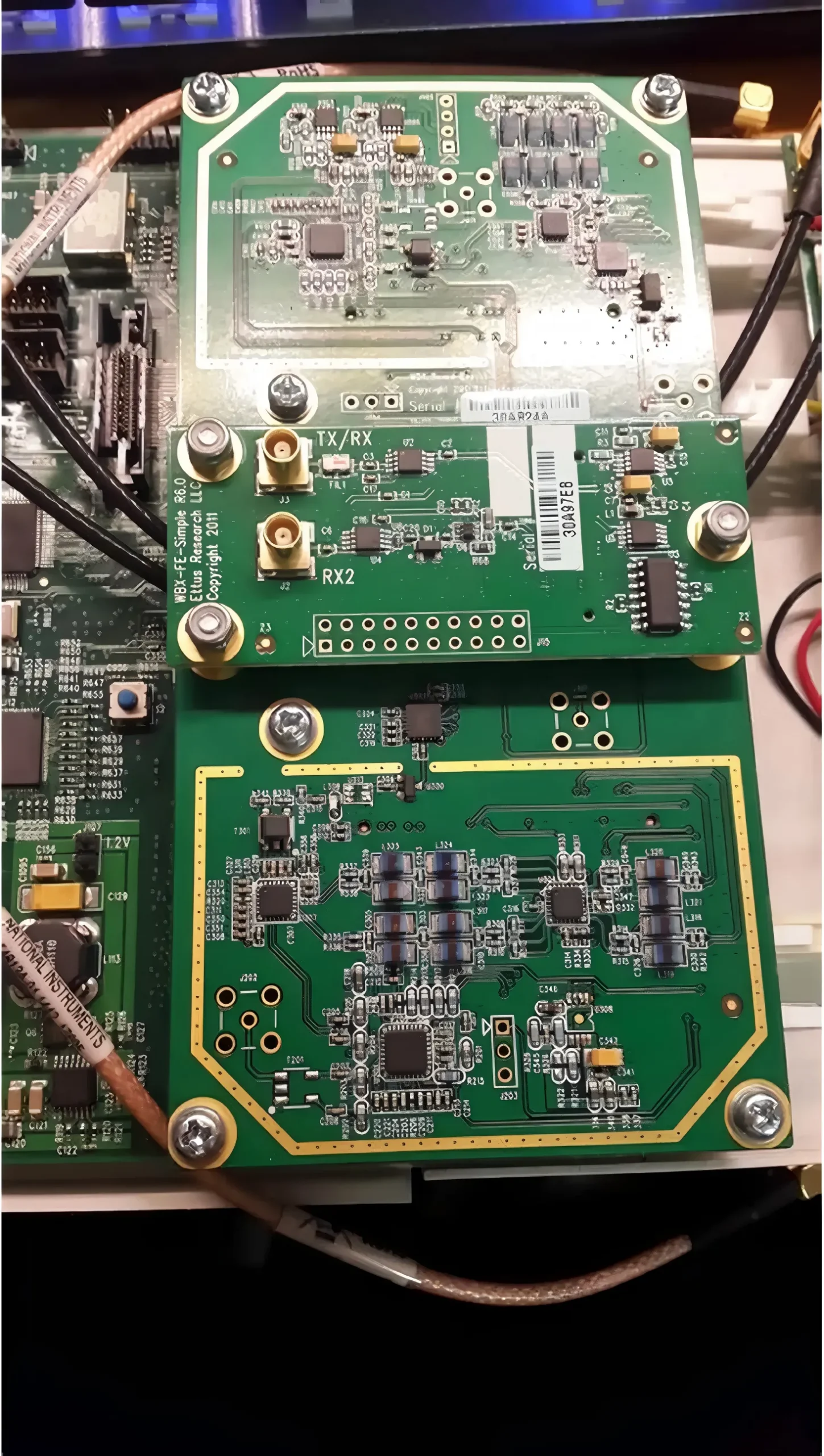
The context for Figure 1 (Page 3) begins by stating that in many RF designs, connector selection is often delayed, leading to misunderstanding of the SMP connector. It is rarely a boundary interface but an internal one, meant to survive tolerance, movement, and imperfect alignment inside dense assemblies. Therefore, this figure should be a system-level architecture schematic. It might show a block diagram of an RF subsystem, where several key functional blocks (e.g., “PA Module,” “Filter,” “LNA Chain,” “Front-End Board,” “Stacked RF Mezzanine”) are highlighted. The interconnections between these blocks are specifically labeled as SMP interfaces, not SMA. The image might visually contrast SMA/SSMA external ports on the device enclosure with these SMP internal interconnects inside. The core purpose of this figure is to establish, at a conceptual level, the application positioning of SMP: it is not a user-accessible “port” but an “internal bridge” engineered to work in controlled environments, setting the stage for subsequent in-depth discussion of its mechanical and electrical characteristics.
In many RF designs, connector selection feels almost administrative. The radio works, the antenna is chosen, the enclosure is mostly defined—and only then does the connector appear on the schematic. That late arrival is exactly why the SMP RF connector is often misunderstood. It is rarely a boundary interface. It is an internal one, meant to survive tolerance, movement, and imperfect alignment inside dense assemblies.
An SMP interface typically lives between RF blocks that are already electrically sensitive: PA modules feeding filters, LNA chains linking front-end boards, or stacked RF mezzanines that must mate blindly during final assembly. In these locations, the connector is no longer just a mechanical joiner. It becomes part of the RF path, the mechanical compliance system, and the manufacturing tolerance stack—simultaneously.
Treating an SMP RF connector as interchangeable with threaded interfaces like SMA connectors often leads to subtle failures. SMA assumes fixed geometry and controlled torque. SMP assumes misalignment will happen and builds limited forgiveness into the interface. When designers align the connector choice with that reality, SMP becomes an enabler rather than a liability.
Identify typical SMP RF connector roles in RF chains
Inside RF signal chains, SMP RF connectors usually occupy short, controlled links rather than long runs. You’ll see them between a power amplifier and a filter block, between a shielded RF daughtercard and a baseband board, or inside modular radios where the RF front end is separated for tuning or variant control.
These locations share a few characteristics. First, they are mechanically constrained. Board spacing is dictated by enclosure height or stacking hardware, not by connector preference. Second, they are electrically sensitive. Any mismatch, excess loss, or coupling shows up immediately in system metrics like EVM, sensitivity, or spurious emissions.
In these roles, SMP is less about convenience and more about controlled compromise. Its push-on mating avoids torque-induced stress. Its floating structure absorbs small offsets that would otherwise load solder joints. But it does not eliminate the need for discipline. The connector only performs as expected when its intended role in the RF chain is clearly defined.
Distinguish board-to-board vs cable-based SMP RF connector usage

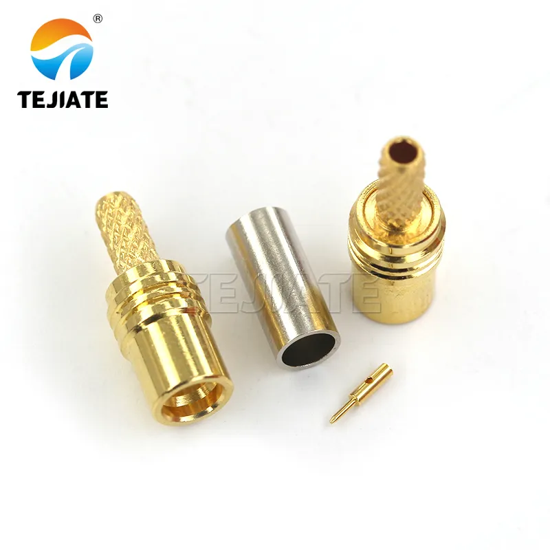
This figure appears at the beginning of the section discussing the distinction between board-to-board and cable-based SMP usage. Its context aims to establish a fundamental understanding of SMP. Therefore, it is likely a standard product photo or simplified cross-section of an SMP connector. The image would clearly show the connector's overall外形 and highlight its non-threaded, push-on snap interface feature. If it's a cross-section, it might schematically depict a floating contact or spring structure to explain how it absorbs axial or radial misalignment. The core function of this figure is to establish a visual anchor, giving readers a concrete impression of “what an SMP looks like,” laying the groundwork for subsequent comparisons with SMA, MMCX and in-depth discussion of its mechanical properties. The image may have only basic annotations, such as “SMP Connector,” “Push-On Interface.”

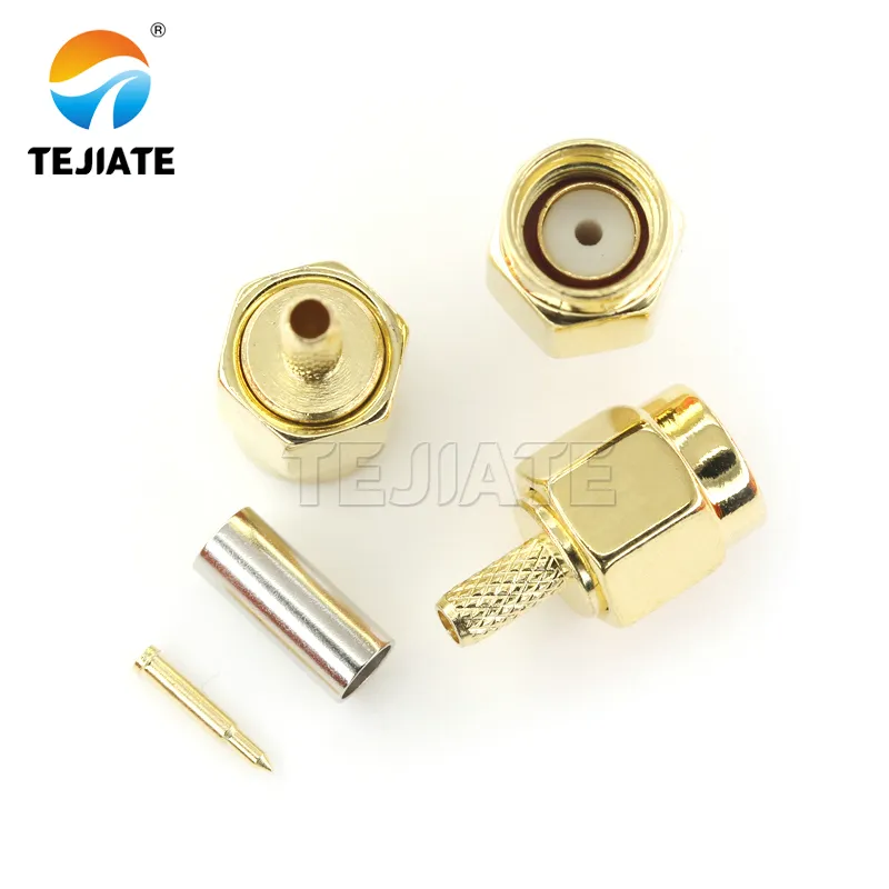
This figure is located within the chapter comparing SMP, SMA, and MMCX connectors. The surrounding text directly analyzes scenarios where SMP outperforms SMA. Therefore, this figure should be a clear illustration of a typical SMA connector. The image would emphasize SMA's external threads and matching hex nut, which visually represent its requirement for wrench tightening. Annotations might include “Threaded Coupling,” “Requires Torque Control,” or “Near-Zero Float.” When juxtaposed with Figure 2 (SMP), this figure aims to provide a visualized feature contrast: on one side is the philosophy represented by SMA—“large size, tool-required, rigid connection”; on the other is the philosophy represented by SMP—“compact size, tool-free, fault-tolerant connection.” This contrast helps readers intuitively understand why SMA might be unsuitable in blind-mate or high-density stacking designs without reading extensive text.

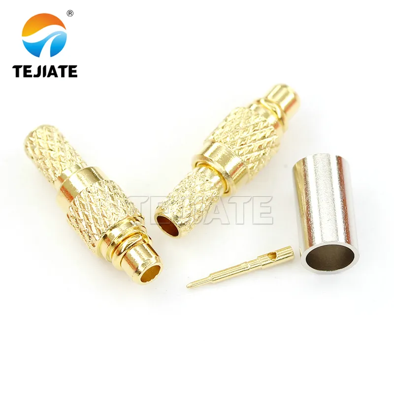
This figure immediately follows Figure 3 and is part of the connector selection comparison. The context states that MMCX is suitable for scenarios where space is extremely tight and mating is manual and controlled. Therefore, this figure is an illustration of an MMCX connector. The image would highlight its even smaller size compared to SMP and its snap interface. Annotations might include “Ultra-Compact,” “For Manual Aligned Mating,” or “Limited Mechanical Compliance.” Together, Figure 2 (SMP), Figure 3 (SMA), and Figure 4 (MMCX) construct a visual representation of a selection spectrum: SMA at one end (robust, stable), MMCX at the other (tiny, manual), and SMP in the middle (compact, floating, blind-mate). This figure helps readers understand that SMP does not solely pursue minimum size but represents a balance point between size, density, and mechanical fault tolerance, fitting applications between where MMCX is too fragile and SMA is too bulky.
One common source of confusion is treating all SMP applications as equivalent. They are not. Board-to-board SMP implementations rely on a three-piece system: two PCB-mounted receptacles and a floating bullet in between. The bullet provides axial and radial compliance, allowing the boards to mate even when spacing or alignment is slightly off.
Cable-based SMP usage behaves differently. Here, the connector terminates a coaxial cable—often RG316, RG178, or a semi-rigid line—and mates to a fixed receptacle. The cable introduces its own stiffness, bend radius limits, and strain paths. The mechanical forgiveness is no longer symmetric.
Designers sometimes assume that because SMP “floats,” a cable-based SMP link will tolerate the same misalignment as a board-to-board bullet system. In practice, the cable often becomes the limiting factor. Understanding which SMP model you are designing around avoids false confidence during layout and assembly.
Decide when SMP beats SMA or MMCX in dense RF modules
Choosing between SMP RF connectors, SMA, and snap-on interfaces like MMCX is rarely about frequency alone. It’s about geometry, access, and tolerance. SMA excels where connectors must be user-accessible, frequently cycled, and mechanically rigid. MMCX works well where space is tight and mating is manual and controlled.
SMP earns its place when neither of those assumptions holds. In blind-mate assemblies, stacked boards, or RF cavities with no tool access, SMP’s push-on mating and float are decisive advantages. Compared with MMCX, SMP offers more forgiveness. Compared with SMA, it dramatically reduces height and assembly effort.
This is why SMP often appears alongside compact RF connector families like MCX in high-density designs, even when frequency requirements could be met by larger interfaces. The decision is rarely about “can it pass RF?” It’s about “will it survive assembly, rework, and life in the field?”
Compare SMP RF connector vs SMA, SSMA, and MMCX before you lock footprints
Benchmark size, frequency range, and mating style
From a purely electrical perspective, SMP RF connectors are commonly specified up to 40 GHz, with higher-frequency variants available in related families. SMA connectors typically support lower practical bandwidth at the PCB launch, while SSMA connectors push frequency higher at the cost of mechanical robustness and ease of handling.
Mating style shapes everything else. Threaded interfaces like SMA and SSMA require torque control and physical access. Push-on interfaces like SMP and MMCX trade that for speed and compactness. In dense modules, eliminating torque tools is often more valuable than squeezing out the last fraction of a decibel.
Insertion life follows the same logic. Threaded connectors tolerate many cycles when torqued correctly. Push-on connectors tolerate cycles only when alignment remains within their design window. Understanding which failure mode you are more likely to face matters more than the nominal cycle rating.
Evaluate mechanical float and blind-mate capability
Mechanical float is the defining feature of an SMP RF connector. Radial and axial compliance allow two imperfectly positioned boards to mate without forcing stress into solder joints or pads. This is the reason SMP appears in blind-mate systems where threaded connectors simply cannot function.
SMA offers effectively zero float. Any misalignment is absorbed by the PCB or the connector body. MMCX offers minimal compliance, but it is not designed for blind-mate stack-ups. In practice, MMCX expects controlled hand insertion.
When blind mating is part of the requirement—even indirectly through manufacturing tolerances—SMP simplifies the mechanical problem. The danger lies in assuming the float is unlimited. It is not. Datasheet limits exist for a reason, and exceeding them turns a forgiving interface into an unreliable one.
Align SMP RF connector choices with SMA / SSMA ports on test and radio gear
Most RF labs and production testers still standardize on SMA or SSMA interfaces. That doesn’t exclude SMP from internal designs. It just means transition planning must be deliberate.
Short SMP-to-SMA or SMP-to-SSMA links preserve test compatibility without bloating internal layouts. The goal is minimizing both electrical length and the number of interfaces. Each additional transition adds uncertainty, especially at higher frequencies.
If you already rely heavily on threaded RF interfaces elsewhere in the system, aligning SMP usage with those expectations—through well-chosen adapters rather than ad-hoc cables—keeps characterization repeatable and debugging sane.
Design SMP RF connector board-to-board links around stack-up and float
Board-to-board SMP links look deceptively simple on block diagrams. Two boards, one connector path, no cable. In practice, this is where most SMP-related issues are born. The reason is not RF theory—it’s geometry. Stack height, tolerance accumulation, and mechanical compliance dominate outcomes long before insertion loss becomes visible on a network analyzer.
An SMP RF connector used in a board-to-board configuration behaves less like a plug and more like a constrained mechanical system. The floating bullet only performs as intended when the surrounding dimensions are designed around it. If the nominal spacing is off, or if tolerances stack unfavorably, the connector may still mate—but outside its optimal electrical region.
That’s why stack-up design deserves the same rigor as impedance control. Ignoring it is equivalent to routing a transmission line without defining its reference plane.
Plan stack height and pad locations for SMP bullets and receptacles

The three-piece SMP system—two receptacles and one bullet—assumes a specific operating window. Datasheets define a nominal board-to-board spacing along with allowable compression and extension ranges. Those numbers are not suggestions. They describe the region where contact geometry, spring force, and impedance alignment are all simultaneously valid.
Designers sometimes set the nominal spacing equal to the mechanical drawing and assume the float will absorb everything else. In reality, PCB thickness tolerance, connector placement tolerance, and assembly variation all push against that margin.
Pad placement matters just as much. Off-center launches, asymmetric ground pads, or uneven solder volumes can tilt the receptacle slightly. At low frequencies, that tilt may be invisible. At higher frequencies, it can introduce repeatable but puzzling return-loss ripple that disappears only when the stack is disassembled.
Control impedance through launch geometry and ground stitching
An SMP RF connector does not magically preserve impedance through a poor launch. The transition from connector pin to PCB trace must be treated as a controlled discontinuity, minimized through geometry rather than hope.
Good practice mirrors what is already established for coaxial launches: consistent reference planes, short signal stubs, and well-placed ground stitching vias. The difference is scale. SMP footprints compress these elements into a smaller area, leaving less room for error.
A useful mental model is to treat the SMP launch as a very short coax-to-microstrip transition. Return current wants the shortest, cleanest path. When the reference plane is broken or vias are sparse, that path lengthens—and mismatch appears. This is not unique to SMP; it is a general RF principle documented across connector families, including those summarized in the broader history of RF connectors.
Budget radial and axial misalignment for reliable blind mating
Blind-mate designs fail when tolerance is assumed instead of calculated. SMP connectors tolerate misalignment—but only within defined bounds. Rather than treating those bounds qualitatively, it is safer to formalize them into a simple planner.
Information Asset: SMP RF Board-to-Board Stack-Up & Misalignment Planner
| Input Parameter | Description |
|---|---|
| Frequency_GHz | Highest operating frequency |
| Target_VSWR | Maximum allowed VSWR (e.g., ≤1.5) |
| Board_Spacing_nom_mm | Nominal PCB spacing |
| SMP_Float_radial_mm | Radial float from datasheet |
| SMP_Float_axial_mm | Axial float from datasheet |
| PCB_Tol_mm | Combined PCB thickness & fabrication tolerance |
| Connector_Tol_mm | Connector placement tolerance |
Derived calculations
- Board_Spacing_min = Board_Spacing_nom_mm − SMP_Float_axial_mm − PCB_Tol_mm − Connector_Tol_mm
- Board_Spacing_max = Board_Spacing_nom_mm + SMP_Float_axial_mm + PCB_Tol_mm + Connector_Tol_mm
- Max_Misalignment_XY = SMP_Float_radial_mm − Safety_Margin_mm
Outputs
- Pass / Fail indicator against frequency and VSWR target
- Recommended Safety_Margin_mm (typically 0.1–0.2 mm)
Design teams that formalize this early often discover that the connector choice is fine—but the nominal board spacing is not. Adjusting spacing is cheaper than reworking footprints later.
Control RF loss and isolation when SMP RF connectors sit in crowded layouts
Estimate insertion loss from SMP RF connector pairs and short coax links
Insertion loss budgeting often stops at the cable. That’s a mistake. A single SMP RF connector pair contributes measurable loss, especially as frequency increases. When combined with short coaxial segments—such as RG316 used for internal jumpers—the total loss can exceed early estimates.
A practical approach is to treat the link as a series element: connector loss plus cable attenuation scaled by length. This mirrors the loss modeling used for coaxial cables in RF standards literature and keeps expectations realistic.
Loss that appears “mysterious” on the bench is often nothing more than unaccounted connector contribution.
Separate high-power and sensitive nodes around SMP clusters
Dense SMP clusters often sit at the intersection of transmit and receive paths. Without careful layout, high-power signals can couple into sensitive nodes, especially LNA inputs. The result may not be catastrophic failure, but degraded noise figure or unstable calibration.
Spacing helps, but spacing alone is rarely enough. Ground fences, stitched vias, and in some cases thin internal shields improve isolation dramatically. These techniques are standard practice in RF packaging and are consistent with broader electromagnetic compatibility guidance from organizations such as the IEEE.
The key insight is that SMP’s compact form factor does not reduce electromagnetic interaction. It simply compresses it.
Validate isolation with vector network analyzer sweeps before freeze
Before layout is frozen, validate isolation across all SMP paths together. Measure not only S11 and S21 for individual links, but also coupling terms between adjacent channels. These cross-terms often reveal layout-driven problems that individual measurements miss.
Catching a −35 dB coupling issue during prototype is manageable. Discovering it after enclosure tooling or regulatory testing is not. Early VNA sweeps pay for themselves quickly.
Specify SMP cable and SMP RF connector pairs for lab and production harnesses
Choose between semi-rigid, conformable, and RG316-style flexible cables

Semi-rigid cables offer excellent repeatability and low movement-induced variation. They are ideal for production harnesses that will not be reworked. Flexible options like RG316 tolerate motion, reassembly, and probing, making them better suited for lab environments.
The trade-off is loss and stability. Flexible cables exhibit slightly higher attenuation and are more sensitive to bend radius. The correct choice depends on whether mechanical adaptability or electrical rigidity is the priority.
Match SMP RF connector interfaces to SMA and SSMA test equipment
Most RF test infrastructure assumes SMA connectors or SSMA connectors. SMP-based designs must bridge that gap cleanly. Short, well-characterized adapters or cables preserve measurement integrity without forcing the internal design to conform to external hardware constraints.
The goal is not zero adapters—it is controlled adapters. Keeping transitions predictable simplifies calibration and troubleshooting.
Avoid common assembly mistakes that kill repeatability
SMP cable assemblies fail most often due to basic mechanical errors: over-bending near the connector, improper solder wetting, or strain applied to the dielectric. These issues rarely appear immediately. They surface after temperature cycling or handling.
Clear assembly instructions and simple inspection criteria prevent the majority of these failures. Repeatability comes from discipline, not exotic materials.
Plan for thermal, vibration, and blind-mate margins in SMP-based modules
Most SMP-related problems don’t show up during bring-up. They appear later—after temperature cycling, after transport, after the enclosure has been opened and closed a few times. That timing is what makes them frustrating. On the bench, the SMP RF connector looks fine. In the system, it slowly drifts toward the edge.
The reason is simple. SMP relies on contact geometry and spring force, not threaded preload. That makes it compact and blind-mate friendly, but also more sensitive to changes in alignment, material expansion, and mechanical stress. None of that is theoretical. It happens in normal products.
Designing margin into the system is not about making the connector stronger. It’s about making the environment less hostile.
Derate SMP RF connector behavior under temperature cycling and shock
Connector datasheets describe performance under controlled conditions. Flat boards. Room temperature. Clean mating. Real systems rarely meet all three at once.
Temperature cycling changes more than electrical length. It changes contact pressure. Different materials expand at different rates, and the SMP interface is where those differences converge. Over time, return loss may degrade slightly, then stabilize, then degrade again. Engineers often misinterpret this as “measurement noise.”
Shock and vibration add another layer. Micro-motion at the contact interface can modulate impedance just enough to matter at higher frequencies. Not enough to fail hard. Enough to erode margin.
The practical takeaway is not to panic—it’s to derate expectations. If your RF budget barely closes at room temperature, it will not improve after environmental exposure.
Choose detent style based on environment, not preference
SMP RF connectors are available in smooth bore, limited detent, and full detent variants. On paper, this looks like a minor mechanical option. In practice, it changes how stress flows through the assembly.
Smooth bore versions insert easily and place minimal load on the PCB. They work well in instruments, lab modules, and systems that are assembled once and left alone. Full detent versions resist vibration better, but they transmit higher insertion and extraction forces into solder joints and pads.
Problems start when detent style is chosen by habit. A full detent connector in a tight blind-mate stack can overconstrain the system. A smooth bore connector in a high-shock environment can walk out of position over time.
Neither option is “better.” The environment decides.
Use structure, not solder joints, to absorb mechanical stress
SMP float is not a shock absorber. It corrects misalignment. It does not carry load.
In systems exposed to vibration, shipping shock, or repeated handling, relying on the connector alone is risky. Mechanical fixtures—brackets, guide pins, enclosure ribs—should define board position first. The SMP RF connector should follow, not lead.
Designs that get this right tend to be boring in the best way. The connector sees alignment, not force. The solder joints see RF, not mechanics.
Qualify SMP RF connector performance in prototypes and production test
Define S-parameter checks that reflect system risk
For most SMP paths, S11 and S21 across the operating band are enough. The goal is not to prove the connector’s theoretical limits. It’s to verify that the assembled system behaves consistently.
Over-testing can be counterproductive. Sweeping to extreme frequencies or chasing datasheet maxima often introduces variability unrelated to real use. Focus on the band that matters.
Threaded interfaces like those discussed in established SMA connector design references are often used as benchmarks, but the same discipline applies here: measure what you need, the same way, every time.
Use time-domain tools when frequency plots stop explaining behavior
When frequency-domain data looks “almost right” but systems still misbehave, time-domain tools help. TDR reveals impedance steps caused by launch geometry, partial mating, or asymmetric stack-up.
In multi-channel designs, time-domain views also expose path-to-path skew that frequency plots can hide. Two links can show similar insertion loss yet differ meaningfully in delay.
These tools don’t need to be part of routine testing. They are most valuable during prototype validation, when design decisions are still reversible.
Establish production go/no-go criteria that actually scale
Production testing is about filtering defects, not characterizing physics. The criteria should reflect that.
Information Asset: SMP Production Acceptance Checklist
- Visual check: connector fully seated, no visible damage
- Electrical check: continuity only, no RF sweep
- RF spot check: return loss ≤ −15 dB at maximum operating frequency
- Mechanical check: insertion force within expected range
This approach won’t catch subtle degradation. It will catch bad assemblies. That’s the point.
Troubleshoot SMP RF connector issues without dismantling the system
Recognize patterns that point to SMP misalignment
Certain symptoms repeat across products. Measurements that change when pressure is applied. Performance that shifts after thermal soak. Units that pass test, fail in the field, then pass again on the bench.
These are not random. They usually indicate partial mating or float overrun. The connector still works—but not in its intended geometry.
Use substitution and bypass to isolate the fault
Replacing an internal SMP link with a known-good external jumper is often faster than speculation. If performance stabilizes, the problem is localized. If it doesn’t, look elsewhere.
This method mirrors troubleshooting approaches used with other compact RF interfaces, including snap-on systems described in practical MMCX connector application guides. The interface changes, the logic does not.
Know when layout fixes stop helping
There is a point where small fixes stop paying off. If misalignment budgets are routinely exceeded, or if frequency targets stretch the connector beyond comfortable margin, a larger change is warranted.
That change might be a footprint adjustment. It might be moving to a related family such as SMPM. The mistake is delaying the decision while symptoms accumulate.
Track SMP RF connector trends that affect future designs
Higher-frequency variants are trading tolerance for bandwidth
SMPM and Mini-SMP push usable frequency higher by tightening geometry. The cost is reduced mechanical forgiveness. These interfaces thrive in controlled assemblies and struggle in forgiving ones.
Designs that anticipate this trade-off early are easier to migrate later.
Non-magnetic SMP variants are no longer niche
Leave room for change
Final engineering perspective
An SMP RF connector is not fragile, and it is not foolproof. It is precise. Designs that treat it as a precision interface—mechanically and electrically—tend to age well. Designs that treat it as a convenience feature tend to accumulate unexplained problems.
Most SMP failures are not connector failures. They are expectation failures.
Fix the expectations early, and the connector rarely becomes the limiting factor.
Bonfon Office Building, Longgang District, Shenzhen City, Guangdong Province, China

A China-based OEM/ODM RF communications supplier
Table of Contents
Owning your OEM/ODM/Private Label for Electronic Devices andComponents is now easier than ever.
