ESD Protection Devices for Embedded Systems
Jan 20,2026
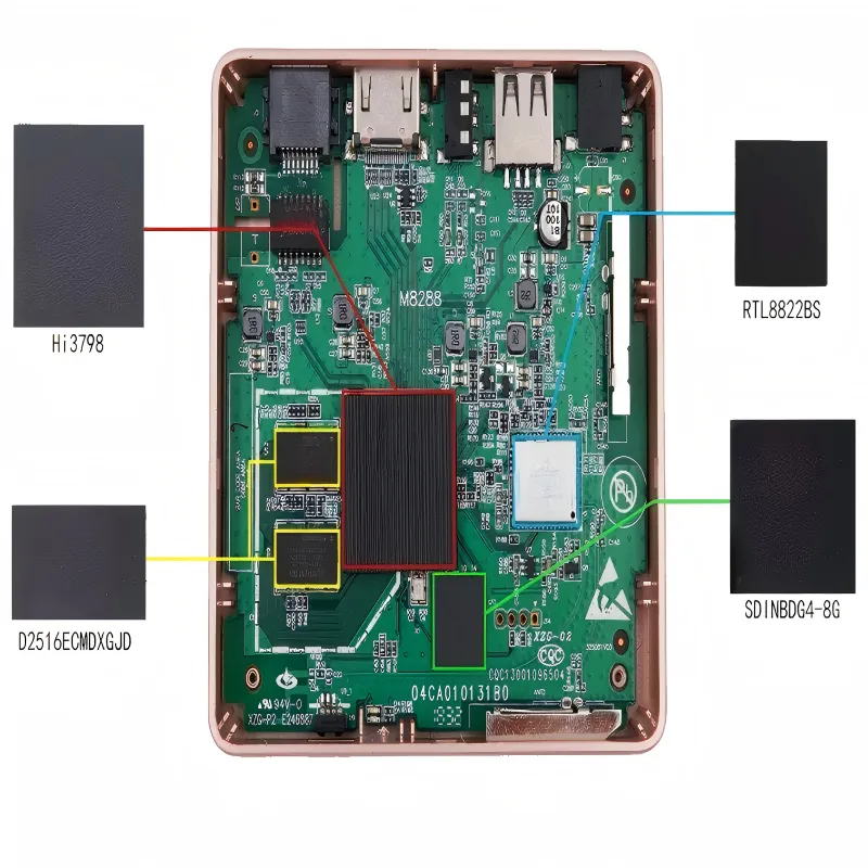
This image appears at the beginning to visually introduce the core challenge of ESD in embedded systems—the stealthy and misleading nature of its failures. It might show a seemingly normal embedded device (e.g., a development board or product prototype) but overlay visual elements暗示 instability: for instance, a flashing “Unexpected Reset” log entry on a screen, a sporadic spike in a waveform graph representing analog sensor output, or a USB connection status icon toggling between “Connected” and “Disconnected.” This image aims to echo the text: “Engineers chase firmware timing, buffer overruns, or power sequencing issues—often for weeks—before realizing the root cause was electrical stress.”
Electrostatic discharge rarely shows up as a clean, dramatic failure. No smoke. No obvious damage. The board powers up, firmware runs, and early validation looks fine. That’s exactly why ESD problems in embedded systems tend to linger longer than they should. Most teams encounter ESD indirectly. A controller resets once every few days. A sensor output jumps under dry conditions. A USB port disconnects only when someone touches the cable shell. Engineers chase firmware timing, buffer overruns, or power sequencing issues—often for weeks—before realizing the root cause was electrical stress, not software logic.
This article focuses on device-level ESD decisions for embedded hardware: when external protection becomes necessary, how discharge energy really enters a product, and how to group protection devices into practical families instead of guessing part numbers. If you are looking for board-level routing patterns and mixed-signal layouts, that topic is covered separately in ESD Protection Circuit Design for Mixed PCBs.
When do embedded systems need dedicated ESD protection devices?
Recognize real products that quietly fail because of ESD, not firmware bugs
Most commercial and industrial embedded products reference IEC 61000-4-2 for ESD immunity. The standard defines contact discharge levels up to ±8 kV and air discharge levels commonly reaching ±15 kV. These tests are applied to real interfaces—connectors, housings, exposed metal—not directly to silicon pins.
That distinction is critical. Internal IC ESD ratings are designed to survive handling during manufacturing. They are not meant to absorb repeated gun strikes through long cables or metal enclosures. Passing IEC testing is a system-level requirement, not a chip-level one. This gap explains why relying solely on internal IC protection is no longer sufficient in modern embedded products.
Decide where internal IC ESD cells stop being enough for modern boards
As semiconductor geometries shrink, on-chip ESD structures shrink with them. Human Body Model and Charged Device Model ratings that once looked generous now sit much closer to minimum safe limits. At the same time, product expectations have moved in the opposite direction. IEC Level 4 immunity is common even in cost-sensitive designs. Automotive and industrial platforms often demand even higher robustness across wide temperature ranges.
Once a signal leaves the PCB through a connector, internal protection alone becomes a liability. External devices are designed to clamp earlier, divert current more effectively, and absorb repeated stress. That is why modern designs treat external ESD protection as a system requirement, not an optional add-on. For MCU pin–level strategies, see ESD Protection for Microcontroller I/O.
Map where ESD hits your embedded product and how energy flows
Trace ESD entry points on cables, connectors, housings, and test pads
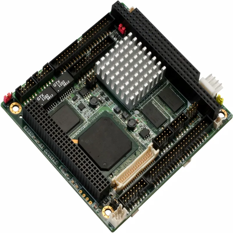
Following the subheading “Trace ESD entry points on cables, connectors, housings, and test pads,” this should be a well-annotated schematic or product photo of typical embedded hardware (e.g., an industrial control board with a heatsink or a compact IoT device). It uses arrows, circles, or highlighted areas to clearly indicate all locations that could be touched by a human, tool, or charged cable: various I/O connectors (USB-A, RJ45, SMA), power jacks, metal buttons, enclosure seams, grounding screws, and programming/test headers or pads. This image visually interprets the simple rule: “if it is touchable, it is a potential discharge point.”
ESD does not appear randomly on a PCB. It enters through physical contact points—places where a charged human, tool, or cable can touch the system. Typical entry points include USB, HDMI, Ethernet, RF connectors, push buttons, exposed test pads, and programming headers. Metal housings and shielded connector shells are especially common strike locations during IEC testing and real-world use.
A simple rule applies: if it is touchable, it is a potential discharge point. If you cannot clearly identify where ESD enters your product, protection decisions become guesswork.
Follow ESD current paths into ground, supply rails, and signal nets
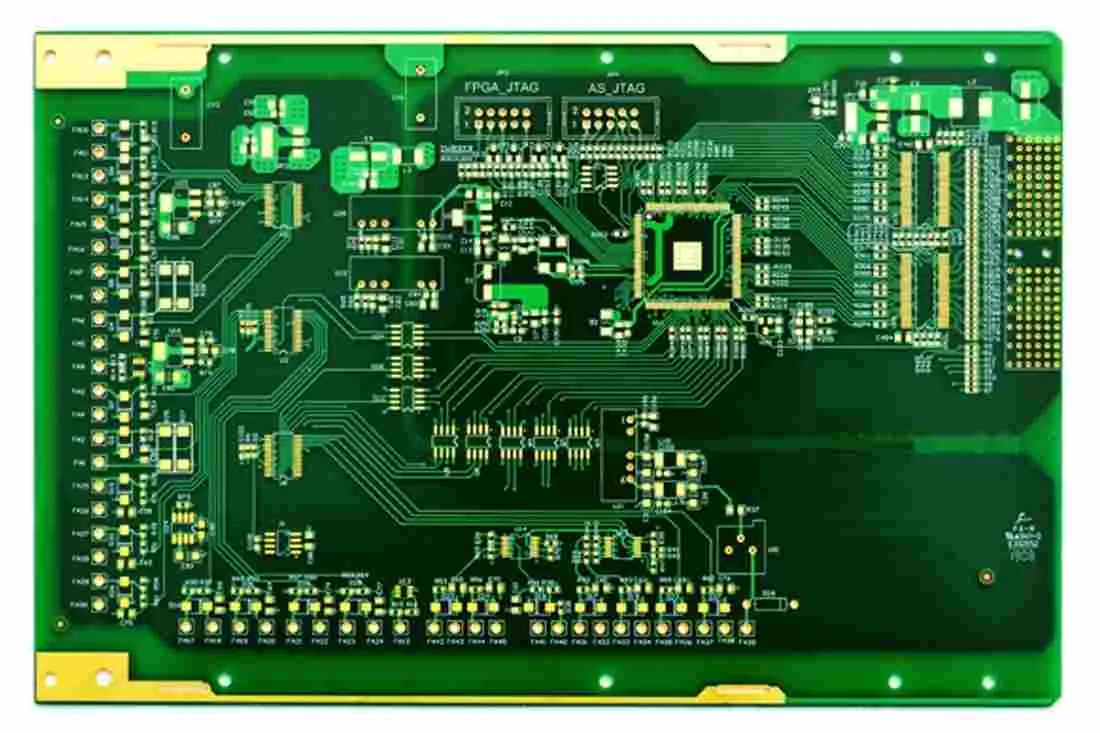
This image follows the subheading “Follow ESD current paths into ground, supply rails, and signal nets.” It is likely a simplified PCB stack-up diagram or layout view that visualizes the energy flow of an ESD event using colored arrows or current lines. The diagram might show: an ESD pulse injected into the metal shell of a USB connector at the top-left; a thick arrow representing the primary current path into a nearby “Chassis GND” pad; however, a set of thinner arrows or field lines indicate how energy couples through parasitic capacitance into the adjacent “Digital GND” plane and “+3.3V” power plane; eventually, this coupled energy appears near an ADC input pin of a microcontroller at the bottom-right. This image explains why ESD failures often occur far from the actual discharge point.
Once a discharge enters, current looks for the lowest impedance path. In practice, that path is rarely direct. ESD energy may flow from a connector shell into chassis ground, jump into digital ground, couple into supply rails, and finally reach sensitive signal pins. This is why ESD failures often show up far from the connector itself.
A poorly placed protection device can force current through long PCB loops, raising local voltages purely through inductance. Understanding current flow—not just placing parts—is what separates designs that barely pass lab tests from those that survive years in the field.
Classify which zones need strong TVS diodes and which only need small ESD diodes
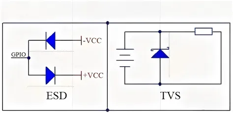
Following the subheading “Classify which zones need strong TVS diodes and which only need small ESD diodes,” this should be an informational zoning diagram that divides a typical embedded system block diagram into two or three main zones. For instance, the left zone might be labeled “Power Input / Long External Cables,” containing symbols for a 12V or 24V power rail and a connector, pointing to a TVS diode schematic symbol with an annotation emphasizing “High Surge Capability.” The right zone might be labeled “High-Speed Data Interfaces (USB, HDMI, Ethernet),” containing differential pair signal lines, pointing to a Low-Capacitance ESD Protection Array symbol with an annotation emphasizing “C < 1pF, Fast Response.” This image clearly argues against using the same protection device for all interfaces.
Not all interfaces experience the same stress. Power rails and long external cables tend to see higher-energy, slower transients. These zones benefit from transient voltage suppressor diodes designed for surge handling. High-speed data lines face a different problem. They require extremely fast clamping and very low capacitance, even if peak current capability is modest.
Treating all interfaces the same is a common—and costly—mistake.
How should you group ESD protection devices into clear families?
Separate signal-line ESD diodes, power-line TVS diodes, and low-capacitance arrays
In practice, most embedded designs rely on three broad protection families. Signal-line ESD diodes prioritize fast response and low capacitance. They are typically used on GPIO, UART, CAN, and LIN lines where bandwidth matters and surge energy is limited. A deeper automotive example is covered in ESD Diode Guide for Automotive CAN & LIN.
TVS diodes focus on higher peak current capability and are commonly placed on power rails and long cables exposed to larger transients. ESD arrays and protection ICs combine multiple low-capacitance channels into a single package, making them practical for dense connectors like USB or HDMI where routing symmetry and PCB space matter. Trying to force one family to protect every interface usually introduces new problems instead of solving old ones.
Explain the key parameters shared across ESD protection devices
Across all families, the same parameters appear repeatedly. Working voltage determines whether the device remains invisible during normal operation. Breakdown and clamping voltages define how much stress reaches the protected IC. Peak pulse current indicates how much energy the device can absorb. Capacitance and leakage decide whether signal integrity or power budgets suffer.
None of these values should be evaluated in isolation. They only make sense when compared directly against the limits of the interface being protected.
Match ESD protection devices to data lines, power rails and connectors
Pair ESD diodes and arrays with high-speed HDMI, USB, and Ethernet ports
High-speed interfaces behave very differently from ordinary digital I/O. USB, HDMI, and Ethernet links are sensitive not only to voltage stress, but also to small changes in impedance and capacitance. A few extra picofarads in the wrong place can reduce eye margin or create link instability that only shows up at higher data rates or temperature extremes.
For these ports, low-capacitance ESD diodes and multi-channel arrays are usually the right tools. Their role is narrow but critical: respond fast, clamp early, and remain electrically quiet during normal operation. In most proven layouts, these devices sit directly at the connector, before any common-mode chokes or filtering networks.
Designers who treat USB or HDMI lines like GPIO often end up with products that technically pass an ESD check but behave poorly in the field. The protection worked. The signal path didn’t.
Select transient voltage suppressor diodes for 5 V, 12 V and 24 V rails
Power rails see a very different stress profile. Hot-plug events, cable inductance, and load switching introduce higher energy and longer pulses than typical signal-line ESD events. Small-signal ESD diodes are not designed for this environment.
This is where transient voltage suppressor diodes belong. TVS devices are characterized for standardized surge waveforms such as 8/20 µs and can conduct significantly higher peak currents without permanent damage. On industrial and automotive rails, they often protect not just against ESD, but against broader transient events as well.
If you want a neutral, non-vendor explanation of how transient suppression differs from classic ESD behavior, the Wikipedia article on Transient-voltage-suppression diode provides a clear technical overview.
Use PESD1IVN27-AX as an automotive CAN/LIN example on embedded boards
Located in the “Use PESD1IVN27-AX as an automotive CAN/LIN example on embedded boards” section, this is likely a close-up screenshot of a real PCB layout or a carefully drawn schematic focusing on the area near an automotive connector. It clearly shows: a multi-pin connector (possibly for CAN_H, CAN_L, power, and ground); for the CAN_H and CAN_L signals, each has a PESD1IVN27-AX (or similar SOD-323 package) device, with one of its pads connected to the signal pin via an extremely short trace (perhaps <2mm), and the other pad connected directly to a large, solid ground plane below via a cluster of multiple vias. A dashed box might outline the “Protection Zone” with an annotation “Place here!”, strongly contrasting the correct placement with the wrong practice of placing the device far from the connector. This image is a concrete embodiment of the idea that “layout matters as much as device choice.”
Automotive communication buses highlight why interface context matters. CAN and LIN operate at higher nominal voltages and are routinely exposed to harsher electrical environments than consumer interfaces. Devices such as PESD1IVN27-AX are designed around those realities rather than adapted afterward.
In practical layouts, this type of protection is placed directly at the network entry point. Not nearby. Not halfway down the trace. Right at the connector edge. The intent is to clamp the event before it propagates into common-mode chokes, termination networks, or the transceiver itself.
A bus-specific discussion of this approach is covered in more detail in ESD Diode Guide for Automotive CAN & LIN.
Decide when a simple single-line device beats a complex protection IC
Integrated protection ICs look attractive on schematics. Fewer components. Cleaner routing. Sometimes better symmetry.
They are not automatically the best choice.
Single-line devices often make more sense when only one or two nets need protection, BOM cost is tightly controlled, or long-term sourcing flexibility matters. They also allow engineers to tune protection strength per line instead of accepting a fixed internal structure.
In many solid designs, the best solution is mixed: arrays where connector density demands them, discrete devices where control and flexibility matter more.
Design around package, layout and parasitics instead of only peak ratings
Understand how SOD-323, DFN, SOT-23 and QFN packages change ESD performance
Datasheet ratings alone rarely tell the full story. Two devices built on similar silicon can behave very differently once mounted on a PCB. Lead length, bond wire geometry, and pad layout all contribute parasitic inductance, which translates directly into higher clamping voltage during fast ESD edges.
This is why small DFN or QFN packages often outperform larger leaded packages in real system tests, even when headline specifications look similar. The difference usually appears during IEC testing, not during schematic review.
Place ESD protection devices to keep loop inductance and ground impedance low
Placement matters as much as device choice. Protection devices should be as close as possible to the discharge entry point, with short, wide connections to ground. Every extra millimeter of trace adds inductance, and inductance becomes voltage during fast transients.
Many borderline ESD failures trace back to layout decisions rather than silicon capability. A “correct” device placed poorly can provide little real protection.
Coordinate ESD devices with filters, common-mode chokes and terminations
Component order is not arbitrary. A common and effective sequence is connector first, then ESD protection, followed by common-mode chokes or filters, and finally the transceiver. Reversing this order often forces ESD current through components that were never meant to handle it.
This interaction between protection and filtering is also discussed in general EMC literature, including the Wikipedia overview on Electrostatic discharge.
How are automotive and high-speed links reshaping ESD protection devices?
Follow the shift from 12 V to 24 V and 48 V automotive nets
Vehicle electrical systems are moving toward higher voltage distribution to reduce current and cable mass. That shift immediately affects protection strategy. Higher working voltage is required, but without excessive leakage or clamping levels that exceed transceiver limits.
Designs that were comfortable at 12 V often lose margin at 24 V or 48 V unless protection choices are revisited early.
Track new ESD protection devices for automotive Ethernet, CAN-FD and camera links
Automotive Ethernet and camera interfaces combine two difficult requirements: very high bandwidth and high immunity. Newer protection arrays focus on lower dynamic resistance and tighter channel matching, often evaluated using system-level models rather than static peak ratings.
Protection is no longer something added after signal integrity is solved. It is part of the signal path from the beginning.
Note market growth and shipment trends in ESD protection devices and TVS diodes
Demand for ESD and TVS devices continues to grow, driven by consumer electronics volume and increasing automotive electronic content. Annual global shipments now reach well into the tens of billions of units.
For engineers, the takeaway is simple: this category is not niche, and device options will continue to expand rather than disappear.
Watch how parts like PESD1IVN27-AX evolve with new assembly sites and PCNs
In long-life automotive and industrial platforms, supply continuity is a real design parameter. Manufacturing changes and additional assembly sites often signal capacity expansion rather than risk.
Teams that monitor these changes early are less likely to face forced redesigns later in a product’s life.
Validate your ESD protection devices with realistic IEC 61000-4-2 tests
Plan gun test setups for ports, housings and cable assemblies
Passing an ESD test starts long before the gun is fired. The most common mistake is testing in a way that does not reflect how the product is actually used. IEC 61000-4-2 defines discharge methods and levels, but it does not tell you where users will touch, which cables will be connected, or what operating modes matter most.
Effective test plans focus on real entry points: connector shells, exposed metal, cable shields, seams in enclosures. Powered and unpowered states should both be tested, and communication links should be active whenever possible. A device that survives a powered-off strike may still fail functionally when traffic is flowing.
For teams new to system-level testing, the standard itself is worth reading carefully, not just as a compliance checkbox but as a guide to realistic stress conditions. Background context on ESD behavior is also summarized well in the Wikipedia article on Electrostatic discharge.
Capture clamping waveforms and functional upsets during strikes
A simple pass or fail result rarely tells the whole story. When possible, measure what happens during a strike. Observing clamping voltage, even approximately, can reveal whether a protection device is turning on early enough or letting excessive voltage reach the protected IC.
Equally important is logging functional behavior. Soft failures—missed packets, transient errors, brief resets—often matter more than hard damage. These events indicate that protection is marginal, even if the hardware survives the test.
Engineers who correlate lab observations with device parameters tend to converge on robust solutions faster than those who only swap parts after failures.
Use lab results to refine device choice, layout and derating rules
Few designs pass demanding ESD tests on the first try. The goal of testing is not just compliance, but feedback. If failures occur, the response should be structured: adjust placement, reduce loop area, change device families, or add voltage margin.
Blindly “adding more protection” often creates new problems, especially on high-speed lines. Iteration, guided by measured behavior, is usually more effective than brute force. For broader board-level strategies, this refinement process is discussed further in ESD Protection Circuit Design for Mixed PCBs.
Solve common ESD protection device questions from embedded engineers (FAQ)
Can one ESD protection device family really cover every connector in a product?
When should I choose a TVS diode instead of a small-signal ESD diode?
How much capacitance is too much for data-line ESD protection?
Can I reuse a USB or HDMI ESD array on automotive CAN or LIN?
Are automotive-grade ESD protection devices overkill for industrial or consumer designs?
How can I fairly compare clamping performance between different vendors’ datasheets?
Closing perspective
Bonfon Office Building, Longgang District, Shenzhen City, Guangdong Province, China

A China-based OEM/ODM RF communications supplier
Table of Contents
Owning your OEM/ODM/Private Label for Electronic Devices andComponents is now easier than ever.
