ESD Protection Circuit Design for Mixed PCBs
Jan 19,2026

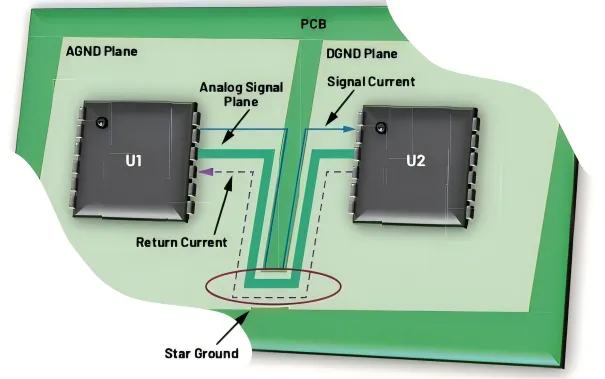
This image appears at the beginning to visually introduce the core difficulty of ESD protection in mixed-signal PCBs—the stealthy and indirect nature of its failure modes. It likely shows a photo or schematic of a PCB containing an MCU, analog front-end, and multiple connectors, but uses visual elements (like a blinking error LED, sporadic waveform glitches, or a text box labeled “intermittent reset”) to暗示 internal instability caused by ESD. The image aims to echo the text description that “the board powers on, firmware runs, interfaces appear functional, but odd behavior surfaces later,” emphasizing the cumulative and systemic nature of ESD damage.
Electrostatic discharge almost never shows up as a clean, dramatic failure on a mixed-signal PCB. There is usually no burnt component, no obvious short, no instant death. The board powers on. Firmware runs. Interfaces appear functional. That is precisely what makes ESD so dangerous in real products. The damage is often cumulative and indirect. A unit works on the bench, passes production test, and even survives early validation. Weeks later, after installation, handling, or repeated cable insertion, odd behavior begins to surface. A controller resets under seemingly random conditions. A communication link drops once a day. An analog reading spikes for no clear reason. In many mixed-signal designs, these are the first signs that the ESD protection circuit strategy was either incomplete or ineffective.
Mixed PCBs amplify this problem because they combine digital logic, sensitive analog paths, external interfaces, and power delivery on the same physical structure. ESD energy entering through a connector rarely stays local. It couples into reference planes, sneaks through return paths, and stresses devices that were never intended to absorb fast, high-energy transients. Engineers who focus primarily on digital design often assume that internal IC protection is sufficient. Engineers with a power background may rely heavily on TVS devices placed on supply rails. In practice, neither approach survives long without a deliberate, board-level view of how ESD actually moves through the system.
This article looks at board-level ESD protection circuit design for mixed-signal PCBs using the same mindset engineers apply to other reliability-sensitive choices. Instead of asking whether a device “has ESD protection,” the focus is on where the energy enters, how it propagates across the board, and how to force it into controlled, low-impedance paths before it interacts with vulnerable circuitry.
When does a mixed-signal PCB really need a dedicated ESD protection circuit?
Many teams treat ESD protection as something that becomes relevant only when compliance testing begins. By that point, the schematic is frozen and the layout is difficult to change. In reality, the need for a dedicated ESD protection circuit is determined much earlier, based on exposure rather than certification. Boards with external connectors, user-accessible metal, long cables, or field installation are operating in an environment where ESD is not an edge case. It is a routine stress mechanism.
One of the most misleading aspects of ESD-related failure is how quietly it manifests. Instead of catastrophic damage, mixed PCBs tend to exhibit intermittent behavior that looks like a system-level problem. Random microcontroller resets triggered by cable hot-plugging, CAN or UART communication errors that disappear after a power cycle, or touch inputs that become unreliable in dry environments are all common examples. These issues are rarely reproducible on demand. They pass factory test and often pass initial validation. As a result, debugging efforts drift toward firmware timing, EMC filtering, or power sequencing while the underlying ESD path remains uncontrolled. In many field returns, the board is technically “functional,” yet no longer reliable.
The gap between internal IC ESD ratings and real-world requirements plays a major role here. Most datasheets specify internal protection levels around 2 kV HBM. Those ratings exist to protect devices during handling and assembly, not to absorb repeated system-level ESD events. Standards such as IEC 61000-4-2 define contact discharges of 8 kV or more, applied through connectors, cables, or enclosure surfaces. These events involve higher energy and much longer current paths. PCB inductance, plane impedance, and enclosure coupling all become part of the discharge. Without external protection, internal ESD structures end up acting as the last line of defense, which is not what they were designed for.
Customer specifications make this even more explicit. Industrial and automotive OEMs often require powered-on testing, defined discharge points, and strict pass criteria that forbid resets or data corruption. Passing these requirements is less about selecting a “stronger” component and more about ensuring that the discharge sees a short, predictable route to ground. This is why many fabrication and design review teams emphasize that layout and current-path control dominate ESD outcomes more than raw device ratings.
Map where ESD energy enters connectors, cables, and enclosures

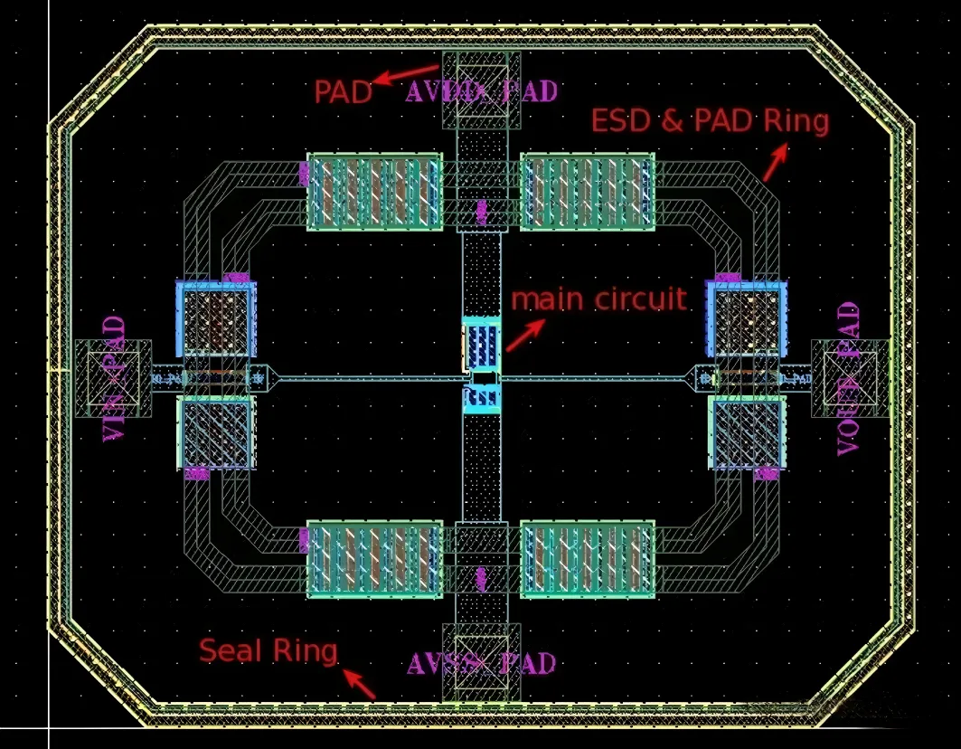
Following the subheading “Map where ESD energy enters connectors, cables, and enclosures,” this should be a detailed schematic or annotated PCB layout of a typical mixed-signal board. It uses arrows, highlighted circles, or callout boxes to pinpoint the physical entry points for ESD: various external connectors (e.g., USB Type-C, RJ45, coaxial antenna port, multi-pin industrial headers), metal mounting posts connected to the enclosure, heatsink attachment points, and test pads for servicing. The image might also distinguish between “obvious entry points” and “less obvious entry points,” emphasizing how poorly terminated cable shields can couple energy into internal signal layers or reference planes.
A useful shift in perspective is to stop thinking of ESD as something that attacks an IC directly. In real systems, ESD enters through the physical interface between the product and its environment. From there, it follows whatever path the design allows. In mixed-signal PCBs, that path is rarely obvious from the schematic alone.
External connectors are the most obvious entry points. USB, HDMI, Ethernet, antenna connectors, industrial I/O headers, and even exposed test pads used during servicing all provide a direct coupling path for discharge energy. Cable shields deserve special attention. While they are beneficial for EMI control, they also provide a low-impedance route for ESD. If the shield termination is poorly defined or relies on long PCB traces, the discharge energy will couple into signal conductors or reference planes instead.
Less obvious entry points often cause more trouble. Metal housings, mounting hardware, heatsinks, and decorative trim can all become discharge locations. In mixed-signal designs, these paths frequently couple into analog ground or sensor reference networks, where even small disturbances can corrupt measurements. Assuming that enclosure design will “handle ESD” without coordinating with the PCB layout is a common and costly mistake.
Once these entry points are identified, each one should map clearly to a protection strategy. The relationship should be straightforward: physical entry point, corresponding schematic node, protection device, and a defined ground return. When this mapping is broken—when signals are routed past protection devices, or when ground returns are indirect—the protection circuit exists only on paper. In practice, ESD will always choose the lowest-impedance path, whether or not that path aligns with the schematic intent.
How should you choose ESD diodes and TVS devices for each interface?

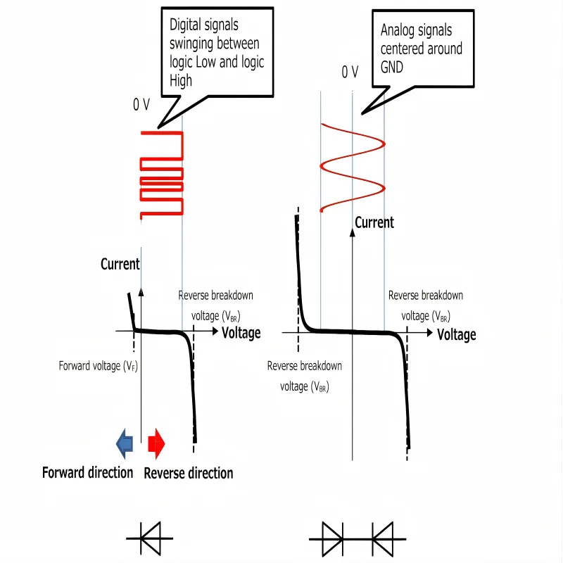
This interpretation focuses on another possible layer of Figure 3—specific parameter matching. The image might contain a table where the left column lists interface cases (e.g., “3.3V, 1MHz SPI”, “12V Automotive CAN”, “480Mbps USB 2.0”, “24V Industrial Analog Input”), and the right column lists corresponding key device parameter recommendations or example values (e.g., VRWM ≥ 5V, C < 3pF; VRWM ≥ 26V, IPP > 5A; C_diff < 0.5pF; Leakage < 100nA). This visually demonstrates the mapping process from “interface characteristics” to “device specifications,” embodying the concept of a “selection matrix.”
Device selection is where mixed-signal ESD design becomes subtle. Different interfaces place very different demands on protection components, and treating them all the same almost guarantees compromise. For logic and data lines, the balance usually revolves around working voltage, clamping behavior, capacitance, and response speed. The protection device must remain invisible during normal operation yet react decisively during a transient event.
Working reverse voltage must exceed the maximum signal level with margin. Clamping voltage must stay below the absolute maximum rating of the protected IC. Capacitance matters more than many designers expect, especially on high-speed or high-impedance lines. Even a few extra picofarads can distort edges, reduce eye margins, or degrade analog bandwidth. Surge current capability must align with the expected stress level, not just the test specification.
Low-speed interfaces such as GPIO, I²C, and UART are generally tolerant of low-capacitance ESD diodes when they are placed correctly. High-speed interfaces are far less forgiving. USB, HDMI, and high-speed Ethernet require protection devices designed specifically for minimal and well-matched capacitance across channels. This selection process is not fundamentally different from other interface decisions engineers already make. Just as you would not use the same cable for RF and power delivery, you should not use the same ESD device across every signal class.
Design patterns used at the pin level scale naturally to the board level. The techniques discussed in ESD Protection for Microcontroller I/O provide a useful foundation, but mixed PCBs require extending that thinking outward, toward connectors, cables, and enclosure interfaces where the energy actually enters.

This image appears near paragraphs discussing the differences between high-speed and low-speed interface protection. It is likely a side-by-side comparison schematic. The left side shows a typical ESD protection circuit for a low-speed interface (e.g., an I2C bus), possibly consisting of just a bi-directional ESD diode and maybe a series resistor. The right side shows a protection circuit for a high-speed interface (e.g., USB D+/D- differential pair), likely using an integrated low-capacitance ESD protection array, with special attention paid to trace symmetry and grounding. Annotations might explain the impact of capacitance (e.g., “C ≈ 5pF, acceptable” vs. “C < 0.5pF, required”), visually demonstrating the different constraints imposed by different signal types on protection devices.
How should you choose ESD diodes and TVS devices for each interface?
Once you know where ESD can realistically enter the board, the discussion changes tone. It stops being about standards and starts being about tradeoffs. Something has to sit between the connector and the rest of the circuit, but there is no neutral choice here. Every protection device changes the electrical behavior of the interface in some way. On a mixed-signal PCB, that change matters.
A common failure mode is over-standardization. One diode family, one footprint, reused everywhere. It looks clean in the BOM and feels safe during schematic review. In practice, it usually means some interfaces are overprotected and others are barely protected at all. Mixed boards rarely punish this immediately. They wait.
Match ESD diode parameters to signal lines and data rates
For simple control lines, ESD diodes are usually straightforward. The signal swings are small, the speed is low, and the tolerance for extra capacitance is generous. As long as the working voltage clears the maximum signal level and the clamping voltage stays below the pin’s absolute maximum rating, the circuit behaves much as expected.
That logic breaks down as soon as the signal carries timing or information density. On analog inputs, added capacitance reshapes the front end in ways that are not obvious from the schematic. On faster digital lines, it quietly eats noise margin. This is why two boards with the same schematic but different ESD parts can behave very differently in temperature or with longer cables.
High-speed interfaces make this even more obvious. USB, HDMI, and similar links do not tolerate generic ESD diodes well, even if they “meet the voltage requirements.” The issue is rarely immediate failure. It shows up as reduced margin, inconsistent enumeration, or sensitivity to cable choice. These problems disappear the moment the protection device is removed, which is usually how teams discover the real cause.
Select TVS diodes for DC power rails and higher-energy surges
Power rails deserve separate treatment, not because they are special, but because they experience ESD differently. When a discharge couples into a supply line, the current lasts longer and the energy involved is much higher than what small ESD diodes are designed to handle. In those cases, TVS devices stop being optional.
A TVS on a 5 V or 12 V rail is not there to “clean up noise.” It exists to define a hard limit on how far the rail can be pulled during a transient event. Capacitance is rarely the limiting factor here. What matters is whether the device can clamp at a voltage the downstream circuitry can survive, and whether it can do so repeatedly without degrading.
What often surprises designers is how indirect this coupling can be. A discharge into a signal pin raises the local ground potential. That disturbance propagates into the supply network through decoupling capacitors and plane impedance. Without a defined clamping point, the rail absorbs stress it was never designed for. This system-level view aligns more closely with how electrostatic discharge is described at a physical level than with the pin-centric view many schematics imply.
Use PESD1IVN27-AX as an automotive IVN example on mixed-signal boards
Automotive and industrial designs remove much of the ambiguity. A mixed-signal board tied to a 24 V vehicle network through external harnesses will see ESD and fast transients whether the designer plans for them or not. CAN and LIN lines are particularly exposed, both electrically and physically.
In that environment, devices such as PESD1IVN27-AX are often used not because they are exotic, but because they sit in a useful middle ground. The working voltage matches the system. The surge capability matches the expected stress. The package allows placement close to the connector, which matters more than most datasheet parameters.
The real lesson is about locality. When the protection device is placed at the edge of the board and tied into a short, low-impedance return path, the rest of the circuit barely notices the event. When that same device is moved a few centimeters inward, the improvement can vanish. On mixed boards, centimeters matter.
Build an ESD protection circuit selection matrix for your PCB
After enough revisions, many teams stop arguing part by part and write their rules down. Not as a checklist, but as a matrix. Each interface gets evaluated once, properly, instead of repeatedly by intuition.
The matrix is usually simple. What is the maximum operating voltage? How exposed is the interface? Can it tolerate added capacitance? Does failure mean inconvenience or hardware damage? The answers point naturally toward low-capacitance ESD diodes, higher-power TVS devices, or sometimes both in series.
Two constraints tend to dominate. The working voltage of the protection device must clear the maximum expected signal or rail voltage with margin. The clamping voltage must stay below the absolute maximum rating of what it protects, leaving room for layout-induced overshoot. Some designers also compare devices using a rough energy estimate for an 8/20 µs pulse, treating it as triangular. It is crude, but it quickly shows which interfaces are being stressed hardest.
Looking at protection devices through the operating principle of a transient-voltage-suppression diode reinforces a point that experienced designers internalize early: these parts do not remove energy. They decide where it goes.
Design ESD protection circuits around controllers, sensors, and analog inputs
Protect microcontroller GPIO, reset, and boot pins without breaking timing
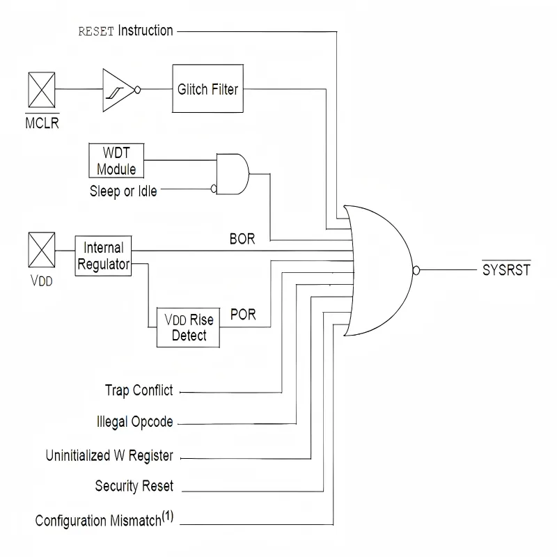
Microcontroller pins are deceptively fragile. GPIO, reset, and boot configuration pins often sit at the edge of the system, connected to buttons, headers, or programming interfaces. These pins are rarely high-speed, but they are timing-sensitive. A poorly chosen protection network can introduce delays or leakage that only show up during power-up or reset sequencing.
A common pattern is to combine a small series resistor with an ESD diode placed near the point of entry. The resistor limits peak current and dampens ringing, while the diode clamps voltage. The mistake is pushing both components too close to the MCU. When the protection device sits far from the connector, the trace inductance between them becomes part of the discharge path, and the MCU pin still sees a large transient. Keeping the protection local to the entry point matters more than matching values perfectly.
Shield analog and ADC inputs from ESD without distorting measurements
Analog inputs present a different set of tradeoffs. These pins are often high impedance, sensitive to capacitance, and tied to reference networks that designers work hard to keep quiet. Adding ESD protection blindly can undo that effort.
In practice, the most reliable approach places the ESD device ahead of any filtering network. The discharge is clamped early, before it can charge the RC elements or inject energy into the reference node. The filter then does what it was designed to do: shape bandwidth and suppress noise during normal operation. When the order is reversed, the filter components end up absorbing ESD energy they were never meant to handle, and the resulting behavior is unpredictable.
Guard low-speed buses like I²C, UART, and LIN using low-capacitance diodes
Low-speed buses are often underestimated because they “work” with almost anything. That tolerance hides a weakness. Long cables on I²C, UART, or LIN lines act as antennas for ESD. Without local clamping, the discharge travels along the cable and arrives at the controller pin with surprising energy.
Low-capacitance diodes are usually sufficient here, provided they are placed correctly. The goal is not to eliminate the transient entirely, but to prevent it from exceeding the bus transceiver’s limits. In mixed-signal boards, this protection often shares ground returns with analog circuitry, which makes placement and routing especially important.
Integrate sensor cable protection with board-level ESD circuits
Sensors connected via external cables blur the line between interface and internal circuitry. Automotive and industrial sensors often carry both signal and power, and their cables are frequent ESD entry points. Treating cable protection and board-level protection as separate problems usually leaves gaps.
The more robust approach is to view the sensor connection as a chain. Cable-side protection limits the initial stress. Board-level protection defines the final clamp and return path. When these two stages are coordinated, the sensor interface behaves predictably even under repeated handling and harsh environments.
Optimize PCB layout so your ESD protection circuit actually works
Keep ESD current loops short between connector, diode, and ground
The effectiveness of an ESD protection circuit depends heavily on loop area. The path from the connector pin to the protection device and back to ground must be as short and direct as possible. Every extra millimeter adds inductance, and inductance raises voltage during fast transients.
Wide copper, short traces, and direct ground connections matter more than elegant routing. This is one of those areas where visual inspection of the layout often reveals problems faster than simulation.
Avoid routing mistakes that bypass the ESD protection path
One of the most common layout errors is routing the signal past the protection device before it is clamped. Another is splitting ground planes in ways that force ESD current to detour through sensitive regions. These mistakes are rarely intentional; they emerge from incremental layout changes and late-stage fixes.
When ESD current finds a lower-impedance path than the protection device, it will take it. The protection component may still be present, but it no longer controls the event.
Coordinate ESD protection with filters, common-mode chokes, and terminations
How can you verify ESD robustness with IEC 61000-4-2 style tests?
Define realistic test points, modes, and failure criteria
Before testing begins, it is worth deciding what “failure” actually means. Is a reset acceptable? Is data corruption allowed if it self-recovers? Which connectors and surfaces are tested? These decisions shape both the test setup and the interpretation of results.
Standards such as IEC 61000-4-2 describe the waveform and severity of discharges, but they do not define acceptable system behavior. That judgment belongs to the designer and, ultimately, the customer.
Capture clamping behavior and soft failures during ESD testing
Not all failures are visible. Many ESD problems show up as brief glitches, communication errors, or state corruption that resolves itself. Logging, instrumentation, and observation during testing often reveal issues that would otherwise be dismissed as noise.
Understanding the discharge behavior also benefits from knowing how the test waveform is defined in IEC 61000-4-2. The standard explains why ESD events stress layouts and protection devices in ways that slow surges do not.
Use test results to refine ESD protection circuit and layout
Compare common ESD protection circuit topologies before locking the BOM
Weigh unidirectional vs bidirectional TVS choices on power and data lines
Evaluate cost, footprint, and assembly risk when adding more protection
Answer practical ESD protection circuit questions from designers
Do I really need an ESD protection circuit if my connectors are shielded?
Can I rely on series resistors alone for ESD protection on I/O lines?
How do I choose between a unidirectional and a bidirectional TVS diode?
What PCB layout mistake most often defeats ESD protection circuits?
How should I budget ESD devices in a cost-sensitive product?
Can I simulate ESD protection circuit behavior instead of testing with a gun?
Is it safe to share one ESD protection circuit between multiple connectors?
Bonfon Office Building, Longgang District, Shenzhen City, Guangdong Province, China

A China-based OEM/ODM RF communications supplier
Table of Contents
Owning your OEM/ODM/Private Label for Electronic Devices andComponents is now easier than ever.
