ESD Diode Guide for Automotive CAN & LIN
Jan 18,2026
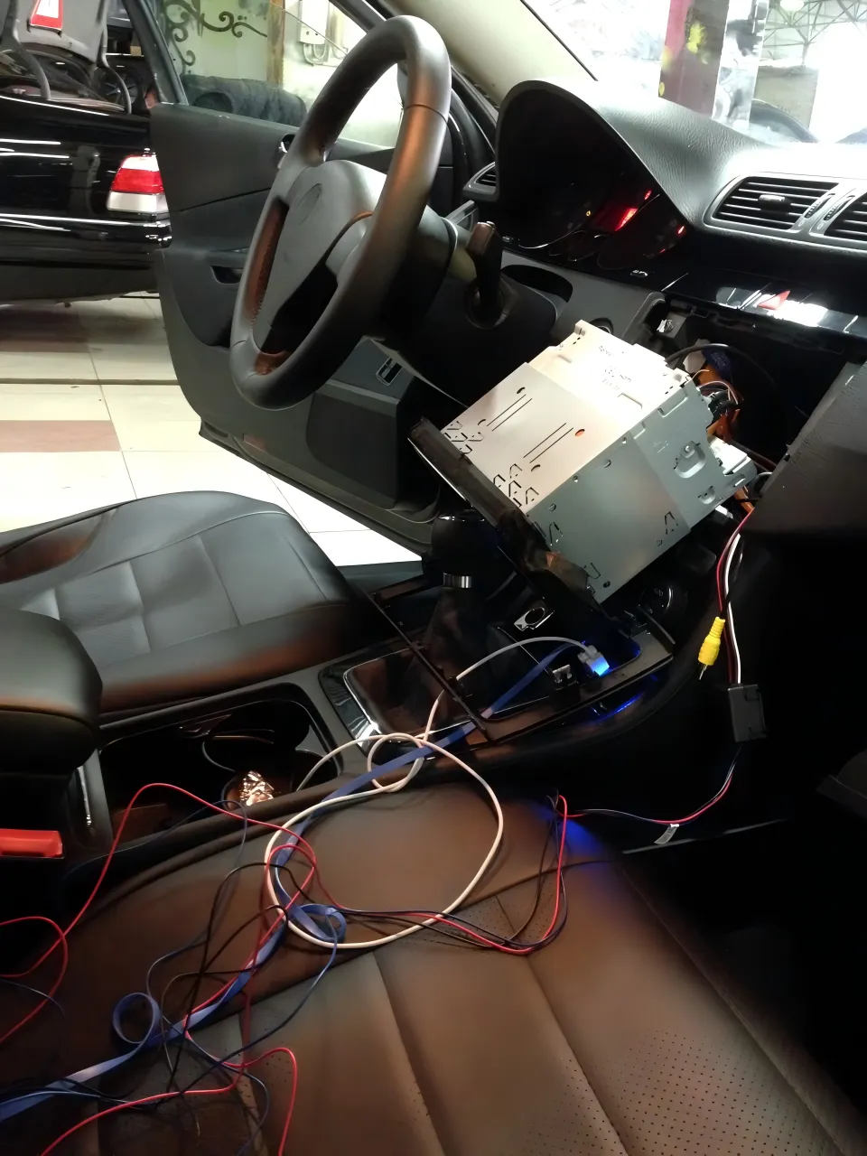
This image appears at the beginning to visually introduce the core dilemma of automotive ESD protection—the delayed manifestation of problems. It might depict a scenario: an ECU that worked fine on the lab bench suddenly experiences communication faults (e.g., CAN bus error frames) or transceiver failure after being installed in a vehicle with longer harnesses. The image may contrast a “clean lab setup” with a “complex vehicle environment” to emphasize the difference in ESD stress conditions, echoing the text about “the harness gets longer” and “a connector is plugged in during a dry winter morning.”
In automotive electronics, the ESD diode is rarely a headline component. It doesn’t define performance, it doesn’t move BOM cost in a visible way, and it usually appears late—often after the CAN or LIN interface already works on the bench.
That timing is exactly why ESD problems tend to surface late as well.
On a clean lab setup, a CAN node may run for weeks without a single issue. Then the harness gets longer. The ECU is mounted to the vehicle body. A connector is plugged in during a dry winter morning. Suddenly, communication errors appear, or worse, a transceiver fails outright. When engineers trace the root cause, it often leads back to how ESD stress was handled—or ignored—at the interface.
This article focuses on ESD diode selection and placement for automotive CAN and LIN, not as an abstract EMC topic, but as a practical design decision that directly affects validation results and long-term reliability.
Clarify when an automotive design really needs an ESD diode
Why IVN lines see more ESD stress than you expect
On paper, CAN and LIN signals don’t look particularly dangerous. Voltage swings are modest. Currents are limited. Many transceivers even advertise “integrated ESD protection,” which gives a sense of security early in the design.
That sense doesn’t always survive first contact with a real vehicle.
Unlike on-board GPIOs or short digital buses, in-vehicle network (IVN) lines leave the PCB. They run through wire harnesses that may be several meters long. Those harnesses are handled by people, routed across metal structures, and exposed to airflow and vibration. All of that contributes to charge buildup.
A long cable behaves like a capacitor whether you intend it to or not. During handling or assembly, static charge accumulates on the harness. When the connector is finally mated to the ECU, that charge looks for the lowest-impedance path to ground. Very often, that path goes straight through the CAN or LIN transceiver pins.
Grounding doesn’t automatically solve the problem. Vehicle grounding is distributed. ECU ground, chassis ground, and battery ground are not always at the same potential, especially during cranking or transient events. During an ESD strike, those differences amplify stress instead of cancelling it.
This is why CAN and LIN ports tend to see more ESD stress than designers expect, even though the nominal signal levels are low. An ESD diode gives that energy a controlled escape route before it reaches the silicon.
Align ESD diode use with OEM specs and IEC/ISO standards
In automotive projects, protection decisions aren’t validated by good intentions. They’re validated by test reports.
Most OEM requirements eventually reference IEC 61000-4-2 or ISO 10605 for ESD robustness. These standards don’t care whether a failure is “unlikely” in your application. They define test conditions that represent worst-case handling scenarios—and expect the ECU to survive them repeatedly.
The important takeaway isn’t the exact waveform definition or test setup. It’s this: an ESD diode must be chosen with those stress levels in mind, not just with normal operating voltage in mind.
A diode that barely meets nominal voltage requirements but clamps too late can still allow damaging energy into the transceiver. Conversely, a diode with aggressive clamping but poor automotive qualification may pass early lab tests and then fail during OEM validation.
This is why ESD protection decisions on CAN and LIN tend to attract scrutiny late in the program. Once validation starts, it’s already expensive to fix.
Map ESD threats across CAN, LIN, and emerging 48 V networks
Identify ESD entry points on connectors, harnesses, and ECUs
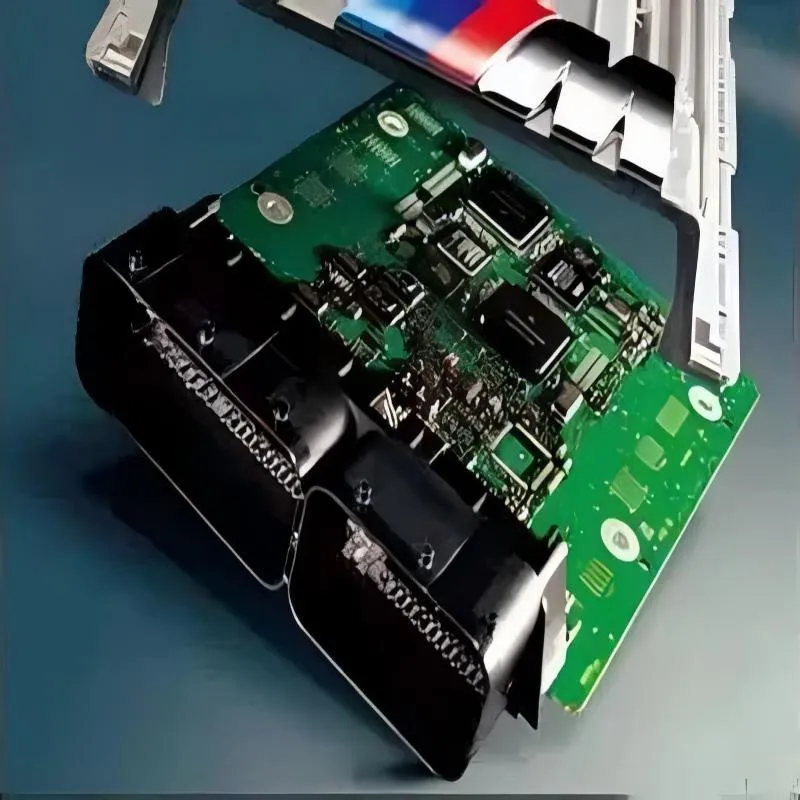
Titled “Identify ESD entry points on connectors, harnesses, and ECUs,” this should be a schematic diagram showing a typical Automotive Electronic Control Unit (ECU) with its connector and the attached harness. It uses arrows, highlights, or labels to pinpoint the physical locations where ESD events are most likely to occur: 1) The metal pins of the external connector (during manual mating); 2) The surface of the harness (triboelectric charging); 3) Any touchable metal parts on the ECU housing. This visually explains why the ESD diode needs to be placed “right at the connector pin.”
ESD doesn’t enter an ECU randomly. It follows very predictable paths once you look at the physical system instead of just the schematic.
The most common entry point is the external connector. This is where humans touch metal, where harnesses meet the ECU, and where different grounding domains come together. Any static charge stored on the cable is discharged at that moment.
From there, the discharge travels along PCB traces unless it is intercepted quickly. If the first protection element sits near the transceiver instead of near the connector, the ESD current already flows across a large portion of the board before it is clamped.
That’s why experienced automotive designers place the ESD diode right at the connector pin, with the shortest possible path to a solid ground reference. It’s not about convenience or symmetry. It’s about stopping the current before it spreads.
This connector-first philosophy shows up across many interface designs, not only CAN and LIN. You’ll see the same logic applied in other signal-protection discussions, such as high-speed I/O protection strategies outlined in broader interface design guides like this overview of cable and interface behavior. Different signals, same physics.
Separate transient types: ESD, EFT, surge, and load dump
Another source of confusion is lumping all transients into a single category.
ESD events are extremely fast. Rise times are on the order of nanoseconds, voltages are high, but total energy is limited. EFT and surge pulses last longer and deliver more energy. Load dump is slower still and tied to alternator and battery behavior.
An ESD diode is optimized for fast response and low parasitic capacitance. It reacts quickly enough to clamp an IEC-style discharge without distorting the CAN or LIN signal during normal operation. What it does not do well is absorb large amounts of energy.
Devices such as PESD1IVN27-AX are designed to handle ESD and limited surge pulses (for example, standardized 8/20 µs currents at a few amps). They are not meant to replace power TVS diodes used on supply rails.
Mixing these roles usually leads to disappointment in validation.
Track industry moves toward 24 V and 48 V communication buses
Automotive electrical architectures are gradually shifting. While 12 V systems remain dominant, 24 V platforms are common in commercial vehicles, and 48 V subsystems are increasingly used in passenger cars to support electrification and efficiency targets.
This shift affects communication networks as well. Higher system voltages increase allowable common-mode voltage on CAN and LIN lines, which in turn pushes designers toward ESD diodes with higher working voltage (VRWM).
At the same time, bus speeds are increasing. CAN-FD places tighter limits on capacitance and signal distortion. The result is a narrower design window: higher voltage tolerance without sacrificing signal integrity.
Semiconductor suppliers have responded by expanding automotive-qualified ESD portfolios aimed at these higher-voltage environments. For designers, the message is clear. Protection strategies that worked for legacy 12 V CAN nodes may not scale cleanly into newer architectures.
Choose ESD diode parameters for 12 V and 24 V bus lines
Match Vrwm, Vbr, and Vclamp to CAN/LIN transceiver limits
A common mistake is to treat VRWM as a simple “greater than battery voltage” requirement. In a real vehicle, CAN and LIN lines rarely see a clean, static reference. Common-mode voltage shifts with ground offsets, harness routing, and operating state. Cold crank, jump-start, and load transients don’t necessarily destroy components, but they stretch the voltage envelope in ways that matter for protection devices.
That’s why many experienced automotive designers don’t select VRWM right at the edge. Instead, they apply a conservative buffer, often approximated as VRWM being about ten percent higher than the maximum expected bus voltage. This small margin keeps the ESD diode from entering conduction during normal operation, even when temperature drift and tolerance stack up in the worst possible direction. It also reduces leakage concerns that can quietly appear late in the program.
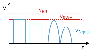
This should be a characteristic curve graph visualizing the most important parameters of an ESD diode. It likely plots a typical diode V-I curve, with voltage on the X-axis and current (possibly on a log scale) on the Y-axis. Three key voltage points are clearly marked on the curve: VRWM (Reverse Stand-off Voltage, the rated voltage where the diode remains in a high-impedance state), VBR (Breakdown Voltage, the point where the diode starts conducting significantly), and VCLAMP (the clamped voltage at a specified high pulse current). This graph visually shows how designers balance between “normal non-operation,” “start of response,” and “effective protection.”
Breakdown voltage, VBR, determines when the diode actually begins to conduct under stress. If it sits too close to VRWM, leakage rises and long-term reliability can suffer. If it is too high, the diode waits too long to react, allowing excessive voltage to reach the transceiver pin. The sweet spot is not a single number; it is a range that complements the absolute maximum rating of the CAN or LIN transceiver.
Clamping voltage, V_clamp, is where theory meets validation. During an ESD event, the question is not whether the diode turns on, but whether it limits the voltage fast enough and low enough to stay within the transceiver’s safe operating window. In practice, engineers usually check that the maximum clamp voltage under the specified pulse current remains comfortably below the IC’s absolute maximum rating, with an additional margin to cover measurement uncertainty and part variation. That margin is what prevents borderline passes from turning into sporadic failures during repeated testing.
Following the subheading “Use an automotive ESD diode selection matrix for CAN/LIN,” and corresponding directly to the table in the text, this image is likely that clear comparison table. Column headers probably include: Bus Type, System Voltage, Max Bus Voltage, Transceiver V_abs max, VRWM_min, VBR range, VCLAMP max, Target ESD Level, Max Capacitance, Package, and AEC-Q101 Requirement. Each row corresponds to different scenarios like LIN, 12V CAN, CAN-FD, 24V CAN, and may provide example parts (e.g., PESD1IVN27-AX). This image is a practical tool for quick selection.
Balance capacitance and leakage with bus speed and EMC margin
Capacitance is often treated as an afterthought until signal integrity problems appear. On LIN, which runs at relatively low speed, capacitance rarely drives the decision. Designers can usually afford a more robust diode without visible impact on communication.
On CAN, especially CAN-FD, the situation is different. Parasitic capacitance on the line directly affects edge rate and noise margin. Too much capacitance can blur transitions just enough to make the bus more sensitive to EMI, even if the design looks fine in early tests. This is one reason why ESD-related issues sometimes surface during EMC validation rather than during basic functional testing.
Leakage current deserves similar attention. A few microamps may not matter in isolation, but modern vehicles contain dozens of ECUs, many of which spend long periods in low-power states. Accumulated leakage across multiple interfaces can influence sleep current budgets and trigger uncomfortable questions late in the design review.
From an EMC standpoint, there is always tension between robustness and transparency. Lower capacitance preserves signal fidelity but can reduce energy absorption capability. Higher capacitance improves clamping robustness but risks degrading the bus. There is no universal answer, only an informed compromise.
Decide when AEC-Q101 grade is non-negotiable for ESD diodes
In theory, any diode that meets electrical requirements could protect a CAN or LIN line. In practice, automotive programs draw a clear line between experimental hardware and production ECUs. For anything destined for series production, AEC-Q101 qualification is rarely optional.
AEC-Q101 does not guarantee immunity to every failure mode, but it demonstrates that the device has survived temperature cycling, high-temperature reverse bias, and mechanical stress tests representative of automotive environments. When an OEM reviews a design, the presence of AEC-Q101 parts on external interfaces simplifies the discussion. Their absence complicates it.
There are cases where non-AEC parts are used intentionally, such as prototypes or internal test fixtures. In those scenarios, the risk is consciously accepted by the team. What matters is understanding that skipping automotive qualification shifts responsibility away from the component supplier and onto the system designer.
For readers who want broader context on why ESD behaves the way it does and why qualification matters, it’s useful to revisit the fundamentals of electrostatic discharge and how repeated stress affects semiconductor junctions over time.
Use an automotive ESD diode selection matrix for CAN/LIN
| Bus Type | Vsys | Vbus,max | VTransceiver V_abs,max | VRWM_min | VVBR Range | Target ESD | Max Cd | Package | AEC-Q101 | Example | V_clamp,max |
|---|---|---|---|---|---|---|---|---|---|---|---|
| LIN | 12 V | ~18 V | ~40 V | ≥20 V | 22-30 V | ±15 kV IEC | ≤15 pF | SOD-323 | Yes | PESD1IVN 27-AX | <45 V |
| CAN | 12 V | ~24 V | ~42 V | ≥26 V | 26-32 V | ±30 kV ISO | ≤15 pF | SOD-323 | Yes | PESD1IVN 27-AX | <45 V |
| CAN-FD | 12 V | ~24 V | ~42 V | ≥26 V | 26-32 V | ±30 kV ISO | ≤10 pF | DFN | Yes | — | <45 V |
| CAN (24 V) | 24 V | ~36 V | ~60 V | ≥40 V | 40-48 V | ±30 kV ISO | ≤15 pF | DFN | Yes | — | <70 V |
Use PESD1IVN27-AX as a concrete design example
Decode PESD1IVN27-AX datasheet specs into real-world limits

On the surface, PESD1IVN27-AX is unremarkable. Its datasheet lists a 27 V working voltage, controlled breakdown behavior, a defined clamping voltage under standardized pulse current, a wide operating temperature range, and a compact SOD-323 package. None of those numbers stand out in isolation.
What matters is how they line up with real CAN and LIN environments. The 27 V VRWM provides headroom for 12 V systems that experience common-mode shifts without forcing the diode into conduction during normal operation. The clamping behavior limits voltage at the transceiver pin during fast ESD events, redirecting current into the ground system rather than through sensitive IC structures. The temperature range ensures that these behaviors remain consistent under under-hood conditions, where consumer-grade parts quietly degrade.
Compare PESD1IVN27-AX with other IVN ESD diode families
Within automotive IVN protection, devices tend to fall into recognizable categories. Single-line ESD diodes emphasize routing flexibility and predictable behavior on individual conductors. Dual-line arrays reduce part count and assembly effort but impose tighter placement constraints.
PESD1IVN27-AX sits firmly in the single-line category. That doesn’t make it universally superior, but it does make it forgiving in early layouts and first revisions, where connector placement and ground strategy are still evolving. In many projects, that flexibility translates directly into fewer late-stage surprises.
Decide where single-line SOD-323 beats dual-line ESD arrays
In practice, single-line devices often win not because of electrical superiority, but because they give designers control. They can be placed exactly where the ESD current enters, routed with minimal stubs, and tied into the most effective ground reference. That control becomes valuable when validation uncovers marginal behavior and small layout tweaks are the only viable fix.
Dual-line arrays make sense when space is constrained and routing is tightly defined from the start. When uncertainty remains, especially in early hardware, single-line ESD diodes offer margin that doesn’t show up clearly on schematics but matters in the lab.
Design PCB layouts that keep ESD diode paths short
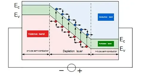
By the time a CAN or LIN design reaches layout, the ESD diode is already chosen and rarely questioned again. That is usually where problems begin. In most post-mortems, the diode itself was not wrong. The placement was. ESD does not behave like a slow transient that politely follows the schematic. It behaves like a fast current impulse that takes whatever physical path offers the least impedance in that instant.
For IVN interfaces, the most reliable layouts follow one rule consistently: the ESD diode must be electrically closer to the connector than to anything else. That means the discharge current sees the diode before it sees trace length, vias, or internal copper pours. When the diode is placed a few centimeters away, the trace between the connector and the diode becomes part of the stress path. At nanosecond time scales, that trace inductance is enough to let the voltage spike exceed what the transceiver can tolerate, even if the diode clamps perfectly on paper.
Grounding is the second half of the same problem. A diode tied to a fragmented or distant ground plane behaves very differently from one tied directly into a solid reference. Designs that consistently pass ESD validation tend to provide a short, wide connection from the diode pad into a continuous ground plane, often reinforced with multiple vias. This is not about DC resistance. It is about minimizing loop inductance during the first few nanoseconds of the event.
Common mistakes show up repeatedly in failed layouts. Long stubs between connector and diode are one. Routing the diode return through a narrow ground neck is another. Placing the diode next to the transceiver for routing convenience is probably the most common compromise. All of these look reasonable until the ESD gun comes out. Then the difference between a 3 mm path and a 30 mm path suddenly matters.
When common-mode chokes are used, their position relative to the diode matters as well. A robust CAN or LIN layout usually clamps ESD energy first, then lets the choke and termination network handle signal conditioning. Reversing that order exposes more of the network to fast transients, even though every individual component still meets its datasheet limits.
Validate ESD diode performance in the lab before SOP
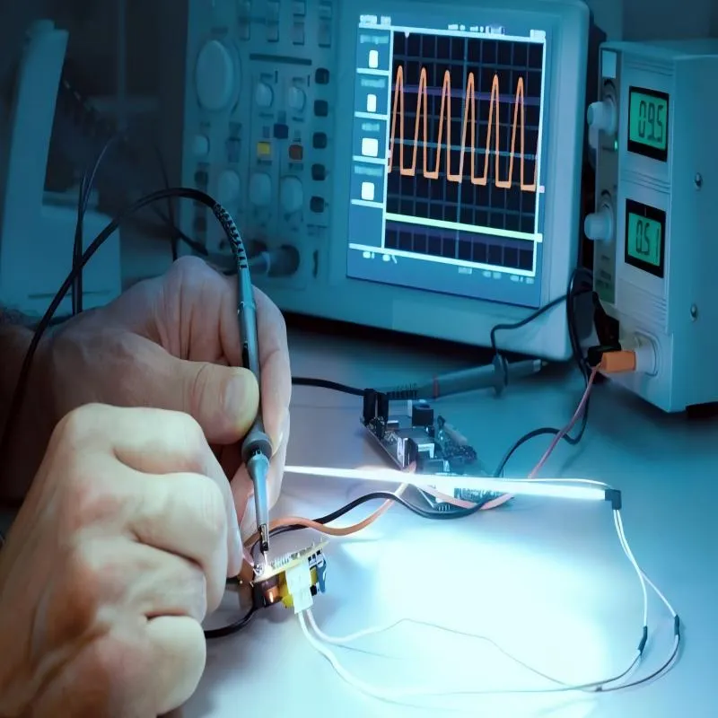
located in the “Validate ESD diode performance in the lab before SOP” section, this should be a photo depicting a real automotive ESD testing scenario. The photo likely includes: an ECU placed on a grounded reference plane; the discharge tip of a calibrated ESD simulator (ESD gun) aimed at a pin of the ECU’s external connector; harnesses connected to the ECU; and test equipment (e.g., a PC, oscilloscope, or bus analyzer) monitoring CAN/LIN bus communication. This image emphasizes the importance of dynamic testing with the system powered and operating to uncover “soft failures” like error frames or resets.
No amount of careful layout replaces validation. In automotive projects, ESD testing is often where designs that looked conservative reveal weak spots. This is not because the tests are unrealistic, but because they deliberately represent worst-case handling scenarios.
A basic in-circuit test setup is usually enough to expose problems. A calibrated ESD gun, a grounded reference plane, and an ECU that is powered and actively communicating on CAN or LIN will show whether protection is effective. Passive testing misses too much. Error frames, bus resets, or unexpected microcontroller behavior only appear when the system is operating.
The most useful data comes from correlation, not repetition. Logging which pin was struck, at what polarity and level, and what the system did immediately afterward makes patterns visible. In some cases, the bus survives but the application resets. In others, communication degrades without a reset. These differences often point to whether the ESD energy was clamped early or allowed to propagate through internal ground structures.
When measurement access is available, probing at the diode pads can be revealing. Seeing how quickly the voltage collapses during a strike often explains why two layouts using the same diode behave very differently. The physics behind this behavior aligns closely with what is described in discussions of CAN bus physical layer behavior, especially when common-mode stress is involved.
For OEM reviews, documenting edge cases matters as much as documenting passes. Showing that the design was exercised across temperature, supply variation, and harness length builds confidence. Even when everything passes, that record reduces follow-up questions and avoids late requests for redesign.
Compare ESD diode, TVS diode, and other protection options
Confusion between ESD diodes and TVS diodes is common, partly because datasheet terminology is inconsistent. Some vendors label fast, low-capacitance devices as TVS diodes, others call similar parts ESD protection diodes. The distinction is not categorical; it is functional.
For CAN and LIN signal lines, the priority is fast response and low parasitics. That is where the typical automotive ESD diode fits. Power TVS diodes, by contrast, are designed to absorb more energy and react on slower time scales. They belong on supply rails, not on communication lines.
MOVs and varistors occasionally appear in discussions of vehicle protection, especially on higher-energy nets. They handle energy well but age with repeated stress and usually lack the stability and qualification expected on IVN signals. Their capacitance and leakage characteristics also make them a poor fit for CAN and LIN. In practice, automotive-grade ESD diodes remain the most predictable and controllable option for these interfaces.
Understanding where each device class belongs avoids the temptation to “overprotect” signal lines in ways that actually reduce robustness.
Practical ESD diode questions that come up late in automotive projects
At some point, usually during layout review or validation, the same questions tend to surface.
One is whether a single ESD diode can protect both CAN_H and CAN_L. In practice, it cannot. A single-line diode only clamps one conductor. Differential pairs require either two discrete diodes or a dual-line array designed for that topology.
Another is whether the same ESD diode can be reused for CAN and LIN. Often it can, as long as the diode meets the stricter of the two interfaces. In most vehicles, that stricter requirement comes from CAN, not LIN.
Placement questions come up frequently as well. The answer is rarely subtle: the diode belongs as close to the connector as possible, not near the transceiver. Moving it “just a little” for routing convenience can be the difference between passing and failing ESD tests.
There is also recurring confusion about using high-speed USB ESD diodes on CAN-FD to save BOM lines. Sometimes it works electrically, but many such devices lack the working voltage range, temperature rating, or qualification required for automotive use. Without careful validation, that shortcut introduces risk rather than reducing it.
Finally, teams often ask how to know whether the ESD diode is actually doing its job in-circuit. The only reliable answer is testing under operating conditions, correlating functional behavior with measured clamp response, and being honest about margins. Paper compliance does not survive contact with an ESD gun.
Frequently asked ESD diode questions in automotive CAN & LIN designs
Can one ESD diode protect both CAN_H and CAN_L lines?
In practice, no. A single-line ESD diode only provides a discharge path for one conductor. On a differential CAN pair, ESD stress can couple differently into CAN_H and CAN_L depending on connector geometry and harness conditions. Protecting only one side leaves the other exposed. That’s why production designs either use two identical single-line ESD diodes, one per line, or a dual-line array explicitly designed for differential buses.
Can the same ESD diode be reused on both CAN and LIN in a vehicle?
Often yes, but only when the diode satisfies the stricter electrical and qualification limits. LIN places fewer demands on capacitance and edge fidelity, so CAN usually defines the minimum requirements. If the diode’s working voltage, clamp voltage, leakage, temperature range, and qualification are acceptable for CAN, it will almost always be acceptable for LIN as well.
Where should the ESD diode be physically placed on an ECU PCB?
As close to the external connector pin as the layout allows, with the shortest possible path to a solid ground reference. Placing the diode near the transceiver instead of the connector allows ESD current to traverse part of the PCB before being clamped, which reduces effectiveness. In validation, that extra path length often shows up as higher peak voltage at the IC pin.
What is the practical difference between an ESD diode and a TVS diode in automotive designs?
The difference is mainly in optimization, not function. Devices marketed as ESD diodes are typically optimized for very fast response and low capacitance, making them suitable for signal lines like CAN and LIN. TVS diodes often emphasize higher energy handling and are intended for supply rails or slower interfaces. The datasheet parameters matter far more than the label.
Is AEC-Q101 certification mandatory for ESD diodes in production vehicles?
For series-production ECUs, it effectively is. Most OEMs expect external interfaces to use AEC-Q101 qualified components, especially on networks that leave the PCB. Using non-qualified parts may be acceptable in prototypes or internal tools, but it shifts reliability and qualification risk onto the design team and often triggers questions during design reviews.
Can a high-speed USB ESD diode be used on a CAN-FD bus to reduce BOM lines?
Sometimes it works electrically, but it is rarely a drop-in substitute. Many USB ESD diodes are optimized for very low capacitance but have working and clamping voltages that do not align well with 12 V or 24 V automotive environments. Many are also not qualified for automotive temperature ranges or stress profiles. Without explicit validation, this substitution is risky.
How can I verify that my ESD diode actually passes IEC 61000-4-2 in the real circuit?
By testing the ECU powered and communicating, not in isolation. Apply contact and air discharges directly at the connector pins using an ESD gun, monitor bus behavior and application-level response, and correlate any resets or error frames with measured clamp behavior at the diode pads. Passing a datasheet rating alone does not guarantee in-circuit robustness.
Bonfon Office Building, Longgang District, Shenzhen City, Guangdong Province, China

A China-based OEM/ODM RF communications supplier
Table of Contents
Owning your OEM/ODM/Private Label for Electronic Devices andComponents is now easier than ever.
