Clamping Diode Design Guide for MCU Inputs and Interfaces
Dec 28,2025
Why do modern MCUs and interfaces still rely on clamping diode solutions?
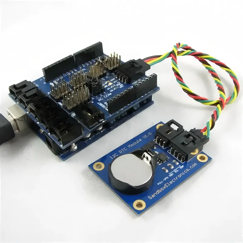
Located in the article's introduction, this figure visually introduces the core issue: on-chip protection is insufficient for real-world sustained overvoltage faults, establishing the need for external clamping diodes.
Open almost any modern microcontroller datasheet and you’ll find a familiar reassurance: GPIO and ADC pins include internal ESD or clamp structures tied to the supply rails. On paper, that sounds like sufficient protection. In real hardware, it rarely is.
Those internal structures are designed for ESD-scale events—very fast, very short, and extremely low energy. They are not intended to absorb sustained fault currents or cable-borne transients. A miswired 24 V sensor, a floating industrial cable, or a hot-plug event can force currents far beyond what on-chip clamps are meant to survive. The result is often subtle rather than catastrophic: rising leakage, drifting ADC readings, or GPIOs that slowly lose drive strength.
External clamping diode networks exist to handle exactly these situations. By adding an external diode (often paired with a series resistor), excess energy is diverted away from fragile silicon junctions and into supply rails or ground paths that are explicitly designed to handle current. Instead of asking the MCU to absorb abuse, the circuit gives that energy somewhere safer to go.
Many engineers only recognize this need after field returns. Boards pass functional testing, firmware behaves normally, and everything looks fine—until months later, when only one channel begins to misbehave. At that point, adding external clamps feels obvious in hindsight.
If you’re already familiar with diode behavior in power and signal paths, the principles here will feel intuitive. If not, it’s helpful to first understand how Schottky devices differ electrically from standard rectifiers, as discussed in this practical overview of Schottky diode applications and design considerations. That context makes clamp design decisions much easier to justify.
How can you quickly map the main clamping diode application scenarios?
MCU, ADC, and op-amp inputs
Digital and industrial interfaces
Power and driver ports
Functional waveform clamping
Not all clamps exist purely for protection. In oscilloscopes, video paths, or radar signal chains, diodes are used to restore DC levels or limit excursions as part of normal operation rather than fault response.
Thinking in these buckets helps narrow the design space quickly, before datasheets and simulations enter the discussion.
How should you read the schottky diode symbol and draw proper clamping topologies?
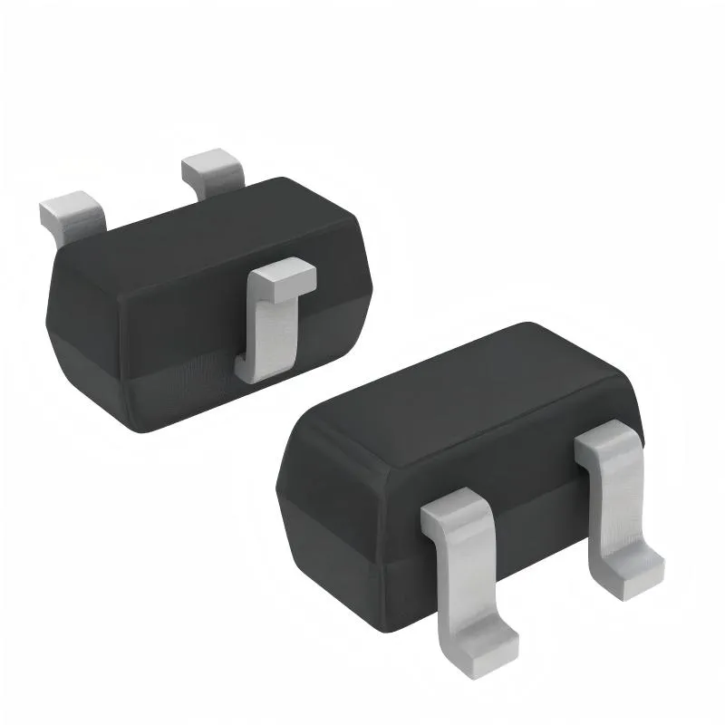
This figure appears in the section “How should you read the schottky diode symbol...”, emphasizing the importance of correctly identifying schematic symbols and PCB package polarity markings to avoid protection failure due to reversed installation.
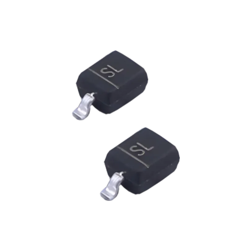
This figure complements Figure 2, further showcasing small-package diodes and introducing the discussion on PCB layout—that clamping diodes should be placed close to the protected pin or connector to ensure a low-inductance path and effectiveness.
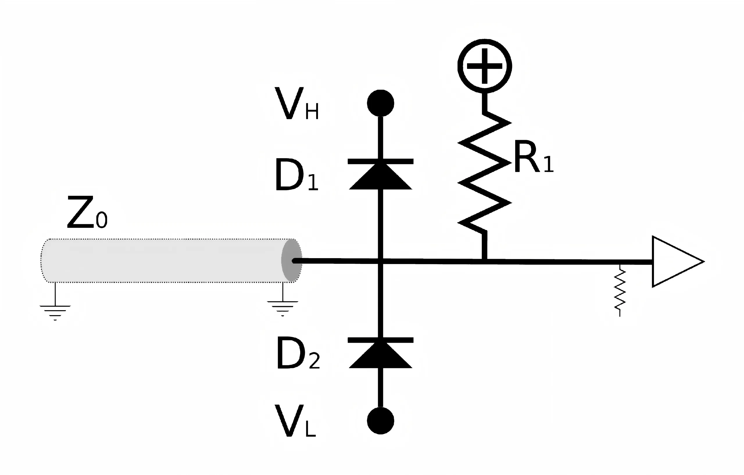
At the schematic level, Schottky diodes look deceptively similar to standard rectifiers. The schottky diode symbol differs only by a subtle change at the cathode, but that small visual cue represents a metal–semiconductor junction with very different electrical behavior.
When used for input or output clamping, the topology is usually simple:
- High-side clamp to VDD
The diode’s cathode connects to the supply rail, and the anode to the signal node. When the signal exceeds VDD plus the diode’s forward voltage, current is steered into the rail.
- Low-side clamp to ground
The orientation is reversed. Negative excursions below ground forward-bias the diode and safely divert current away from the protected pin.
Most MCU inputs use both paths, creating a voltage window that closely mirrors absolute maximum ratings in the datasheet. A series resistor ahead of the clamp limits current so the diode operates safely during fault conditions.
In practice, many clamp failures trace back not to electrical overstress, but to polarity mistakes in small packages. SOD-323 or SOD-523 footprints often have subtle cathode markings, and a mirrored footprint can silently disable protection. Clear schematic symbols and unambiguous PCB silkscreen markings matter more here than many engineers expect.
For designers also dealing with polarity mistakes at the supply level, it’s worth noting that clamp networks often work alongside reverse-polarity protection stages rather than replacing them, as discussed in this reverse polarity protection circuit design guide.
Which schottky diode characteristics actually control clamping behavior and signal distortion?
Located in the section discussing diode characteristics that control clamping behavior, this figure provides a visual complement to the “Clamping Diode Selection and Loss / Distortion Quick Estimator” table, helping engineers quickly understand the trade-offs between different diodes.
If you’ve ever selected a clamp diode purely by voltage rating, you’re not alone—and you’ve probably been bitten by it at least once.
In real designs, clamp behavior is dominated by just a few parameters, and they don’t all show up as red flags during schematic review.
Reverse voltage (Vr) is the obvious starting point, but many failures happen because Vr was sized to nominal conditions rather than credible faults. A 12 V rail is rarely just 12 V in the field. Miswiring, inductive kickback, and cable coupling all stack on top. Seasoned designers usually leave at least a 1.5× margin, sometimes more if the interface leaves the PCB.
Then there’s surge current capability (Ifsm). Clamp diodes don’t fail gracefully here. They often survive dozens of abuse events before leakage creeps up, ADC readings drift, and nobody immediately connects the dots. That’s why peak current ratings matter more than average current in clamp applications.
Forward voltage (Vf) quietly defines how much stress the protected pin actually sees. On low-voltage logic, the difference between a Schottky at ~0.3 V and a silicon rectifier diode at ~0.7 V is not academic—it can decide whether the internal structures ever turn on at all. Vf also sets instantaneous dissipation during a fault, which feeds directly into thermal stress.
Two parameters tend to be underestimated until late testing: leakage current and junction capacitance (Cj). Leakage shows up as offset on high-impedance nodes. Cj shows up as mysteriously rounded edges or lost bandwidth. Neither usually triggers an ERC error, but both show up on the bench.
If you want a broader perspective on how these parameters vary across Schottky families, the discussion in this Schottky diode practical design guide lines up closely with what most engineers see in real hardware.
Clamping Diode Selection and Loss / Distortion Quick Estimator
Interface and fault assumptions
| Input | What it represents |
|---|---|
| Vnom | Normal operating voltage |
| Vfault | Maximum credible fault voltage |
| Rseries | Series resistor or source impedance |
| fsignal | Signal bandwidth or edge speed |
| Load | MCU pin, ADC, op-amp, interface, power |
Typical diode families
| Diode family | Common use | Vf trend | Cj trend | Practical takeaway |
|---|---|---|---|---|
| Signal Schottky | Precision inputs | Very low | Very low | Minimal distortion |
| Fast recovery diode | Switching nodes | Medium | Medium | Handles dv/dt |
| Schottky rectifier diode | Power rails | Low-medium | High | Efficient but "heavy" |
| Rectifier diode | High-energy faults | High | High | Tough, not precise |
First-order checks engineers actually use
- Clamp current estimate
I_clamp ≈ (V_fault − V_clamp) / R_series
- Instantaneous diode stress
P ≈ Vf × I_clamp × fault duty
- Signal impact check
f_cutoff ≈ 1 / (2π × R_source × Cj)
If your signal frequency isn’t comfortably below this, distortion is not hypothetical.
Quick decisions
- Vr too close to V_fault → reject early
- I_clamp near Ifsm → redesign or upsize
- f_signal approaching cutoff → expect edge rounding or gain error
This kind of table won’t replace validation, but it prevents obvious mistakes from reaching layout.
How do you choose between rectifier, Schottky, and Zener clamping schemes on power and high-energy ports?
Once you move to power and driver interfaces, the rules change. Precision becomes secondary. Energy management takes over.
A classic rectifier diode clamp is blunt but reliable. High Vf, high surge tolerance, and very little subtlety. It won’t clamp tightly, but it will survive abuse that would quietly kill a small-signal device.
A schottky rectifier diode lowers losses and heat, which matters when faults aren’t rare. In systems that see repeated hot-plug or brownout conditions, this difference shows up quickly on thermal images.
The schottky diode vs zener diode question usually comes down to intent. Zeners impose an absolute ceiling. That’s useful, but it comes at the cost of dissipation and dynamic resistance. Many robust designs let a Schottky steer current first, then rely on a Zener or TVS element to absorb energy without overstressing the rail.
Fast recovery diode options appear where switching speed matters—SMPS inputs, motor drives, and noisy industrial environments. Reverse recovery behavior there directly affects EMI and switching loss.
In practice, power-entry protection is layered. Clamps work alongside polarity protection, bulk TVS devices, and layout strategies. If you’re already designing that front end, the approach outlined in this reverse polarity protection diode design guide aligns well with how clamp networks are usually integrated.
How can you design small-signal clamping diodes for MCU, ADC, and op-amp inputs without killing accuracy?
This is the point where many protection schemes quietly fail. Not electrically—numerically.
On paper, clamping an MCU or ADC input looks trivial. Add a diode to VDD, another to ground, and call it done. In practice, precision inputs behave like unforgiving critics. They notice everything: leakage, capacitance, even layout-induced asymmetry.
The first decision is almost always the series resistor. It limits clamp current, but it also interacts with the input sampling network. Too small, and the diode sees excessive stress during a fault. Too large, and acquisition time stretches, especially on SAR ADCs. There is no universal value, but engineers usually start by bounding fault current first, then checking whether the ADC still settles within one LSB.
Next comes the diode itself. For small-signal paths, a low-leakage Schottky often outperforms a generic signal diode, even if both meet voltage requirements. Leakage current is the hidden offender here. A few microamps flowing through a high source impedance can shift readings enough to trigger calibration drift complaints months after deployment.
Capacitance matters just as much. Junction capacitance forms a pole with the source resistance, and that pole doesn’t announce itself loudly. Instead, it shows up as “why does this channel look slower than the others?” on a scope. Engineers who’ve debugged this once tend to become very conservative about Cj on precision inputs.
If you’re already protecting polarity at the system level, these clamps usually work alongside that circuitry rather than replacing it. In many designs, the combination mirrors what’s described in this reverse polarity protection circuit design guide, just scaled down for signal-level energy.
How should you place clamping diodes on a PCB to balance ESD robustness, EMI, and serviceability?
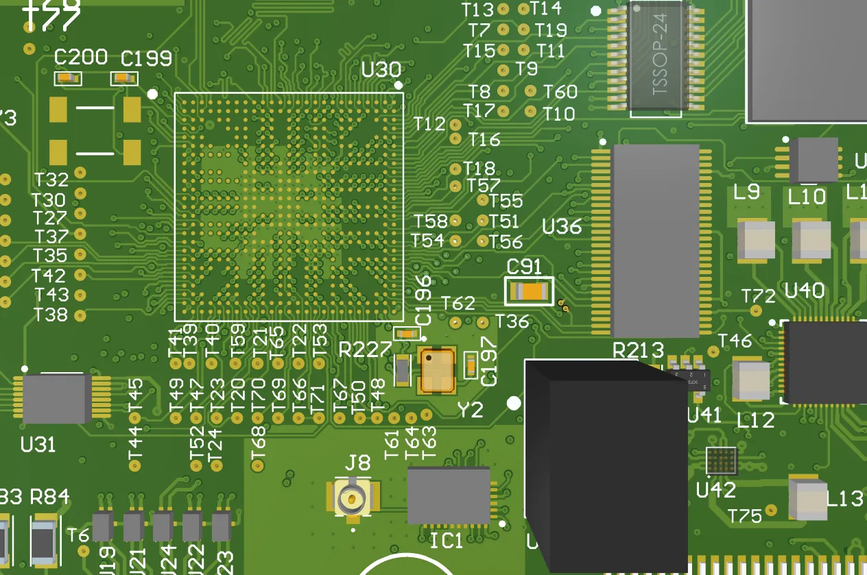
This figure is located in the chapter discussing emerging trends at the end of the article, visually summarizing the higher demands placed on clamping protection in modern designs: lower capacitance, higher reliability, and a layered design philosophy.
A well-chosen clamp can be made ineffective by a careless layout. This is where theory stops helping.
The rule engineers repeat—because it’s earned—is simple: short loops win. The current path from connector to clamp to return must be as tight as possible. Long traces add inductance, which raises the actual clamp voltage right when you least want it to.
Another practical rule: keep clamp currents out of sensitive ground regions. It’s tempting to tie everything into the nearest ground pour, but when a transient hits, that return path becomes noisy. Analog references and clock returns should not share copper with clamp currents if it can be avoided.
Clamps also need to cooperate with TVS devices. TVS elements usually sit near the connector and absorb bulk energy. Local clamping diodes near the IC then fine-limit the voltage to something the silicon can tolerate. When designers skip one stage and expect the other to do everything, reliability suffers.
Finally, think about the poor person debugging this board a year from now. Clear polarity markings, visible reference designators, and accessible test points turn a half-day fault hunt into a ten-minute confirmation.
How do you validate clamping diode designs in the lab and during production?
Protection that isn’t tested is protection you’re only hoping works.
In the lab, validation doesn’t need to be dramatic. A programmable supply or source-measure unit is enough to inject controlled overvoltage while you watch clamp behavior on a scope. What matters is not just the clamp level, but how quickly it engages and how hot the diode gets during repeated events.
ESD testing adds another layer. Watching the waveform during an IEC-style discharge often reveals surprises—ringing, overshoot, or unexpected coupling paths. Those observations are more valuable than a simple pass/fail result.
Production validation tends to be quieter but just as important. Many teams implement a reduced-energy overvoltage check as part of incoming or final inspection. The goal isn’t to stress parts, but to confirm that protection paths are intact and behaving as designed.
Engineers who tie these acceptance criteria back to their original clamp calculations tend to catch issues early, before they turn into field returns.
What new ESD and overvoltage protection trends around clamping diodes are emerging in USB-C and automotive systems?
Two domains are pushing clamp design harder than most others: high-speed consumer interfaces and harsh automotive environments.
USB-C and multi-gigabit links leave almost no margin for added capacitance. Protection devices now need extremely low Cj while still clamping tightly enough to protect sensitive PHYs. This has driven the rise of integrated protection arrays that combine steering diodes and TVS structures in carefully matched layouts.
Automotive systems push in a different direction. Temperature, lifetime, and ESD severity dominate. Clamps must survive years at elevated temperature while tolerating repeated high-energy events. As a result, multi-stage protection—TVS for energy, Schottky clamps for precision, and resistors for current limiting—has become the norm rather than the exception.
The common lesson across both fields is that a single clamping diode is rarely sufficient on its own anymore. Robust designs layer protection intentionally, instead of relying on one component to do everything.
FAQ
How do I size a clamping diode and series resistor for a 3.3 V MCU input exposed to 24 V faults?
Start by limiting fault current with the resistor, then confirm the diode’s surge rating and dissipation under worst-case duty.
When should I use a Schottky clamp instead of a Zener or TVS?
Use Schottky clamps when rail-referenced limiting and low capacitance matter; Zeners and TVS devices excel at absorbing energy.
Are internal MCU clamp diodes ever sufficient on their own?
Only for ESD-scale events. Cable faults and miswiring almost always require external protection.
How much signal distortion can a clamp introduce on analog inputs?
Enough to matter if junction capacitance and source resistance push the cutoff near your signal bandwidth.
What is the most common PCB mistake with clamping diodes?
Long return paths that let transient currents contaminate sensitive ground regions.
How do automotive requirements change clamp selection?
Higher temperature ratings, stricter qualification, and multi-stage protection become mandatory.
What failure modes appear when clamps are underrated?
Gradual leakage increase, shifted thresholds, or latent damage that surfaces long after deployment.
Final note
Bonfon Office Building, Longgang District, Shenzhen City, Guangdong Province, China

A China-based OEM/ODM RF communications supplier
Table of Contents
Owning your OEM/ODM/Private Label for Electronic Devices andComponents is now easier than ever.
