Logic Level MOSFET in 12 V Load Design & SOA Practice
Nov 9,2025
How do you verify a MOSFET is truly “logic-level” at 5 V?

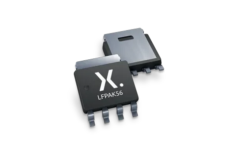
The figure reflects the document’s guidance: a device is “logic-level” only if its datasheet lists Rds(on) at 4.5–5 V (e.g., BUK9Y29-40E), and its Qg/Ciss allow clean switching with 5 V logic.
Not every MOSFET labeled “logic-level” behaves as such when you actually drive it at 5 V. In the lab, you’ll often find devices that promise low Rds(on) on paper but require 8–10 V to reach it. For a real 5 V gate, the only way to be sure is to check the datasheet’s test conditions, not the marketing note.
A true logic level MOSFET lists its Rds(on) explicitly at Vgs = 4.5 V or 5 V, not just 10 V. Nexperia’s BUK9Y29-40E,115, a 40 V N-channel TrenchMOS™ in LFPAK56 (Power-SO8), is a textbook example. It shows 25 mΩ @ 5 A, Vgs = 10 V, and performs stably even with 5 V logic drive, thanks to its low Qg (5 nC @ 5 V) and moderate Ciss (664 pF @ 25 V).

Echoing the text, a “logic-level” label is not enough; check Qg (~5 nC), Ciss and Vgs(max) (±10 V typical) so that 5 V logic can switch the MOSFET without excessive loss or heat.
That combination means a microcontroller or automotive driver IC can switch it directly without a dedicated gate-driver IC—perfect for compact 12 V load designs. But be careful: “logic-level” doesn’t just mean it turns on. It must deliver your target current without excessive voltage drop or thermal rise. If your board layout or thermal vias are minimal, even a 25 mΩ device can climb fast in junction temperature.
For engineers comparing real devices, check Rds(on) binning at 5 V, review Qg and Ciss/Crss trade-offs, and confirm Vgs(max) (±10 V for this part) fits your drive range. Bench-testing the gate waveform and temperature rise under your 12 V load is the fastest sanity check.
What does the SOA curve actually allow for motor stall and solenoid pulses?
Engineers love to claim “it’s within power limits,” but the SOA curve doesn’t care about average watts—it’s about instantaneous V × I over time. During a motor stall or solenoid release, your logic level MOSFET may face 30 V × 10 A for a few milliseconds. That’s 300 W in a small LFPAK56 package.
The BUK9Y29-40E datasheet rates 37 W (Tc) continuous, yet its single-pulse SOA allows far higher short bursts if you respect pulse duration and thermal impedance (Zθ(t)). You can estimate safe operation using:
Zθ(t) → transient thermal impedance curve
Pd_max = (Tj_max – Ta) / Zθ(t)
For a quick approximation: at 1 ms pulse width, Zθ(t) ≈ 0.2 × θJA (assuming 40 °C/W base), meaning brief pulses can reach ~185 W without exceeding 175 °C junction temperature. But stretch that pulse to 100 ms and you’ll exceed limits fast.
In real 12 V load circuits—think automotive fans or door actuators—the worst stress happens at start-up or reverse polarity transients. To stay within SOA, many engineers derate by 20–30 % for temperature, or use parallel MOSFETs when board space allows.
A good practice: measure drain current at turn-on and turn-off under actual load and confirm pulse energy vs. SOA curve. It’s safer than trusting DC power numbers. TEJTE’s Inrush Current Limiter guide also shows how controlled slew rates reduce such stress dramatically.
How should you size gate drive using Qg and switching losses?
Even in low-voltage systems, switching losses can sneak up on you if the gate drive is too weak. The switching loss per cycle can be roughly estimated as:
Psw = 0.5 × Vbus × IL × (tr + tf) × f
For the BUK9Y29-40E,115, with Qg ≈ 5 nC @ 5 V, you can calculate driver current needs directly:
I_driver ≈ Qg × f
At 20 kHz, you’ll need at least 0.1 mA average drive, but momentary peaks can reach hundreds of mA depending on rise/fall times. A driver that can source/sink > 1 A peak ensures clean edges and avoids the linear region, where MOSFET heat spikes.
When rise and fall times stay under 50 ns and Vbus = 12 V, Iload = 5 A, the switching loss is barely ~15 mW. But if edges slow to 200 ns due to weak drive or high Ciss, losses quadruple.
Beyond power, EMI is another reason to tune gate drive. Too-fast dV/dt can inject noise through parasitic capacitances, especially in small packages like LFPAK56. Use a small series gate resistor (2–10 Ω) or snubber network if needed.
If you’re designing compact automotive load switches, TEJTE’s MOSFET Dual-N Guide explains similar trade-offs in gate charge vs. thermal headroom—a useful cross-read when choosing your driver stage.
LFPAK56 (Power-SO8) on a Small PCB — What Changes Thermally?

The figure illustrates how exposed-clip LFPAK56 benefits from copper pour and stitched vias; practical layouts can cut θJA and keep junction temps safe during pulses.
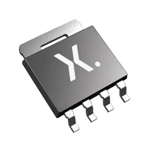
The LFPAK56, also known as Power-SO8, looks small enough to underestimate. But thermally, it’s far from fragile. Its exposed copper clip lets you pull real current—if the PCB helps it breathe.
In datasheets, thermal resistance (θJA) is often quoted under ideal conditions: large copper area, still air, and 1-oz copper. For BUK9Y29-40E,115, θJA ≈ 40 °C/W, yet on a small two-layer board with 300 mm² of copper pour, it may climb to 60 °C/W. Doubling copper thickness to 2 oz or adding thermal vias can cut that almost in half.
Thermal margin shrinks quickly at high load. A 12 V / 5 A circuit dissipating only 0.6 W of conduction loss at 25 °C can push junctions to 70–80 °C in a tight enclosure. When ambient rises to 60 °C, you’re already near 140 °C junction—still safe, but leaving less room for switching or transient events.
Designers often spread the drain pad under the LFPAK56 and stitch 5–8 thermal vias directly beneath. Tie those vias to the ground or drain copper on the opposite layer for heat spreading. This method easily shaves 10–15 °C off Tj at moderate current.
For visual reference, similar thermal spreading practices are discussed in TEJTE’s RF Connector Guide, where heat and impedance balance play the same role in reliability.
How Do You Clamp Inductive Kickback on 12 V Loads — Flyback Diode, TVS, or Both?
When a relay coil, solenoid, or motor is switched off, the stored magnetic energy has to go somewhere. If it can’t flow through the MOSFET, it spikes the drain node and kills your silicon. That’s why every 12 V logic level MOSFET design must have a clamp path.
For slow, low-side drives, a simple flyback diode across the coil is enough—it lets current decay gently and protects the device. But for high-side switches or fast-release applications like ABS valves or latching solenoids, the diode alone can be too slow. That’s where a TVS diode steps in.
Automotive-grade TVS devices, like SMBJ43A or SMCJ58A, clamp around 40–58 V and handle ISO-pulse energies safely. Placed from drain to ground (or across the load), they absorb the initial spike that the flyback diode cannot. For harsh ISO 16750-2 transients such as Pulse 1 (-100 V reversal) or Pulse 5b (load dump up to 87 V / 400 ms), you’ll often need both protection paths.
An automotive TVS diode should be rated for at least 1.5× the normal bus voltage and sized for the pulse energy. Combine that with a fast Schottky flyback diode for controlled decay and clean scope waveforms.
Designers can review TEJTE’s TVS Diode Selection & Testing Guide for a deeper look at ISO pulse shapes, clamp energy ratings, and bench verification methods relevant to automotive switching.
Where Do AEC-Q101 and ISO 16750-2 Matter in a 12 V Load Switch?

The image summarizes the document’s caution: component-level AEC-Q101 (e.g., HTRB, TC, UIS) doesn’t certify your product; system-level ISO 16750-2 pulses (e.g., load dump) still must be passed on the PCB.
It’s easy to assume that using an AEC-Q101 MOSFET automatically makes your design “automotive-qualified.” In reality, AEC-Q101 covers only the component-level stress tests performed by the manufacturer—things like HTRB (high-temperature reverse bias), TC (temperature cycling), and UIS (unclamped inductive switching). A system designer must still prove the entire board passes ISO 16750-2 electrical environment tests.
For the BUK9Y29-40E,115, Nexperia lists full AEC-Q101 qualification, meaning it has survived 1000 hours of HTRB and temperature cycling at 175 °C junction. That doesn’t certify your end product—it just means the transistor won’t be the first point of failure when you start testing.
In vehicle load switching, the bridge between these two standards is critical. AEC-Q101 tells you the device can withstand stress; ISO 16750-2 tells you how severe those stresses can be in the car. Pulse 2a and 2b simulate ignition noise, while Pulse 5b defines load dump energy and timing. If your PCB protection network — TVS, fuse, and filtering — can keep drain voltage below 40 V during those events, a 40 V MOSFET remains safe.
Real-world testing should always include thermal soak and power cycling. Automotive designers often combine MOSFET current monitoring with temperature logging to verify no hot-spot exceeds derated SOA under ISO load profiles. This is where practical benchwork meets paper specs — and where designers earn their reliability.
For context, see TEJTE’s CAN Bus TVS Protection Article for how ISO pulses map to transient energy handling in data lines — the same principles apply to 12 V load switch circuits.
Can You Pass a Quick 12 V Logic-Level MOSFET Check?
Input Fields
- Supply Voltage (VBUS) – Default 12 V
- Load Current (IL) – User value (e.g., 5 A)
- Switching Frequency (f) – e.g., 20 kHz
- RDS(on) @ 5 V & 25 °C = 25 mΩ
- Temperature Coefficient (αR) ≈ 0.4 % / °C
- Qg @ 5 V = 5 nC
- θJA (PCB mount) = 40 °C/W
- Ambient Temperature (TA) – 25 °C typical
Formulas
1. RDS(on) vs Temperature
RDS(on,T) = RDS(on,25) × [1 + αR × (TJ – 25)]
2. Conduction Loss
Pcond = IL² × RDS(on,T)
3. Switching Loss
Psw ≈ 0.5 × VBUS × IL × (tr + tf) × f
or ≈ Qg × Vgs × f
4. Junction Temperature
TJ ≈ TA + θJA × (Pcond + Psw)
5. SOA Check
Verify (VDS, I, tpulse) stays inside the single-pulse curve. If not, derate frequency or increase copper area.
Output Logic
| Result | Action | Suggestion |
|---|---|---|
| Pass | Within SOA | Proceed to layout |
| Derate | Borderline Tj > 150 °C or pulse limit | Add thermal vias / reduce f |
| Fail | Exceeds SOA / VDS | Use parallel MOSFETs or higher Vds rating |
What’s New in Automotive MOSFETs You Should Note in 2024 – 2025?

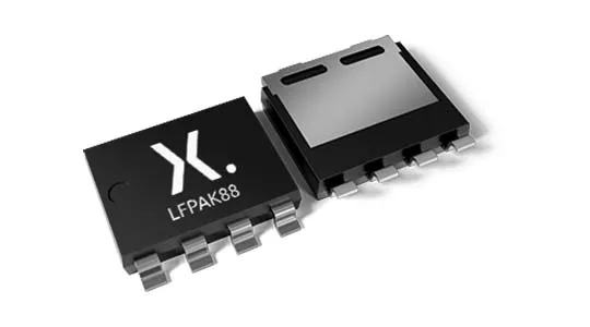
The figure reflects industry trends discussed in the text: newer low-Qg TrenchMOS in compact packages (e.g., LFPAK families) and design flows that validate repetitive-pulse profiles, not just single-pulse SOA.
Automotive power designs are evolving rapidly. Device makers like Nexperia and Infineon are pushing logic level MOSFET performance into even smaller packages such as MLPak and LFPAK88, extending current capacity beyond 100 V domains once reserved for TO-220s.
The BUK9Y29-40E,115 represents this shift — high reliability, AEC-Q101-qualified, and rated up to 175 °C junction temperature while remaining hand-solderable in compact LFPAK56. The industry trend now favors “low Qg, low RDS(on)” trade-offs optimized for 5 V logic drive, ideal for body electronics, lighting modules, and infotainment rails.
Expect broader focus on ISO 16750-2:2023 updates, which define new repetitive-pulse endurance requirements. Designers can no longer validate only single-pulse SOA; they must prove survivability under multi-pulse, high-energy profiles. Bench engineers at APEC 2025 are already demoing adaptive gate-drive controllers that sense temperature and dynamically slow edges to balance EMI vs loss — a sign that power MOSFETs are getting “smarter.”
For compact power stages, TEJTE’s ongoing coverage in its Power Device and Protection Hub continues tracking these packaging and derating trends across the automotive low-voltage space.
Frequently Asked Questions
1.How do I prove a part is “logic-level” without a 10 V gate?
2.Why do designers still fail SOA even when DC power looks fine?
3. Is LFPAK56 big enough for 10 – 20 A loads on a small board?
4. When is a flyback diode sufficient, and when should I add a TVS?
5. Does “AEC-Q101” mean the end product is certified automatically?
6.What changed in load-dump expectations in newer ISO documents?
7.Any 2024–2025 device trends relevant to 12 V loads?

The image mirrors the document’s “quick check” flow: compute Rds(on, T), Pcond, Psw, Tj, then compare (VDS, I, tpulse) to the SOA curve to decide Pass/Derate/Fail and mitigation actions.
Closing Notes
Bonfon Office Building, Longgang District, Shenzhen City, Guangdong Province, China

A China-based OEM/ODM RF communications supplier
Table of Contents
Owning your OEM/ODM/Private Label for Electronic Devices andComponents is now easier than ever.
