IEC 61000-4-2 in Practice: PESD2IVN24-TR for CAN Bus ESD Protection
Nov 8,2025
Which IEC 61000-4-2 level should you target?

This diagram clarifies the IEC 61000-4-2 ESD protection levels to be adopted in automotive electronics design, indicating Level 4 (±8kV contact/±15kV air) as the industry default for automotive ECUs and network nodes, and compares the application of different levels in key modules.
If you design automotive electronics—especially CAN or CAN-FD interfaces—you can’t escape IEC 61000-4-2. It’s the global ESD standard defining how devices must survive electrostatic discharges in real-world handling. But here’s the catch: not every design needs the top rating.
In practice, Level 4 ( ± 8 kV contact / ± 15 kV air ) has become the industry default for automotive ECUs and network nodes. It’s tough enough for production and field use but still practical to test. Lower levels like ± 4 kV might appear in non-critical sensor modules, while infotainment or diagnostic ports often demand the full ± 15 kV air immunity.
To visualize what that means, an 8 kV contact discharge delivers a current pulse of roughly 30 A within the first nanosecond, decaying in about 30 ns. Air discharges at 15 kV can easily double that peak current. This is why your layout and protection network must survive both energy and repetition.
If your board connects to a CAN transceiver such as NXP TJA1042 or TI TCAN1051, IEC Level 4 should be your baseline. Anything less risks random resets or bit errors during real-world plug-in events. (For a deeper standard overview, see IEC 61000-4-2 practical guide on tejte.com.)
What do 8 kV contact & 15 kV air mean on real boards?
Numbers alone don’t tell the full story. On the bench, that ± 8 kV contact test means a 30 ns pulse that dumps energy straight into your connector shell and copper planes. If your return path is narrow, the surge will arc across the gap before your TVS diode ever reacts.
Engineers often expect the “ESD gun test” to behave like a small spark. In truth, it’s a fast LC system with significant parasitics. When the current path stretches across the board, inductance × di/dt can generate several additional volts per centimeter. That’s why layout discipline—short ground paths, perimeter via fences, and solid copper under the connector—is as important as the TVS itself.
Meanwhile, the 15 kV air discharge is a worst-case human-touch scenario. You can pass contact tests on metal connectors yet still fail air discharges on painted bezels or floating shields. For mixed-metal housings, bond every conductive section to a common ground. This advice sounds old-school, but it still saves dozens of validation runs.
Pro tip: In one TEJTE customer design, improving the via spacing from 3 mm to 1.5 mm around the CAN TVS cut the peak transient by >30 %. Such small tweaks often decide a “pass” on the first ESD attempt.
How do system-level vs. device-level ESD differ for selection?
Here’s where confusion often creeps in. Component datasheets quote IEC 61000-4-2 ratings, but that doesn’t mean the whole ECU will pass system-level tests automatically. Device-level qualification (like AEC-Q101) ensures a diode such as PESD2IVN24-TR can withstand the specified waveform at its leads, not after traveling through your board’s parasitic network.
At the system level, every trace, connector, and copper shape reshapes that waveform. A 1-inch stub on a CAN line may reflect part of the surge, turning a 30 A event at the connector into multiple smaller reflections inside the board. That’s why TVS placement and ground return design decide the actual field result.
In short:
- Device-level ESD = lab pulse straight into the diode pins.
- System-level ESD = real gun strike through cables, housing, and PCB structure.
- Pass result = both layers working together.
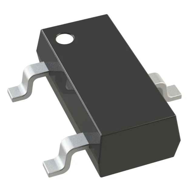
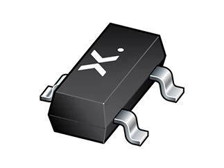
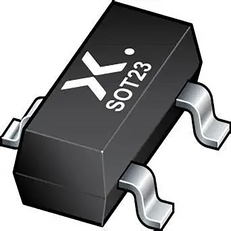
When choosing a TVS, you need both sets of data: the datasheet robustness (IEC Level 4, AEC-Q101) and a clear plan for board-level layout. Nexperia’s PESD2IVN24-TR (24 V VRWM, 42 V max clamp, 14 pF capacitance, 3.5 A @ 8/20 µs, SOT-23 package) fits neatly into this dual view—it’s proven on the device level and layout-friendly for CAN bus symmetry.
You can see similar applications explained on tejte.com/products/semiconductor-devices-2/ under the automotive protection category.
How to map IEC 61000-4-2 to TVS specs (VRWM / VC / C / IPP)

This mapping table provides a practical guide for converting IEC ESD requirements (e.g., ±8kV contact discharge) into key selection parameters for TVS devices (e.g., VRWM, VC, IPP, and C), highlighting the matching parameters of PESD21VN24-TR for CAN bus protection.
When you read IEC 61000-4-2, it only speaks in volts—±2 kV, ±4 kV, ±8 kV, ±15 kV—but engineers buy diodes, not voltage levels. The missing link is how to translate those test levels into the real electrical parameters of a TVS diode: reverse-working voltage (VRWM), clamping voltage (VC), capacitance (C), and peak pulse current (IPP).
At its core, every ESD strike can be viewed as an 8/20 µs surge. The energy delivered can be roughly estimated by integrating the instantaneous voltage–current product,
E ≈ ∫ v(t) · i(t) dt.
In practice, that means if your system must survive ±8 kV contact, you should pick a diode whose VC is well below the transceiver’s absolute-maximum rating, and whose IPP can handle at least 3 – 4 A for the 8/20 µs pulse.
Low capacitance matters too: the total bus capacitance,
Ctot = CTV S + CESD_structure,
affects the CAN-FD eye diagram and signal rise times. Keep Ctot < 30 pF to maintain clean edges.
Below is a practical mapping card derived from real Nexperia data.
IEC to TVS Mapping Card
| IEC ESD Level | VRWM (V) | VC (V @ Ipp) | IPP (A @ 8/20 μs) | Capacitance (pF @ 1 MHz) | Package | AEC-Q101 | Typical Use |
|---|---|---|---|---|---|---|---|
| ±8 kV Contact / ±15 kV Air | 24 | 33–42 | 3.5 | 14 | SOT-23 (TO-236AB) | Yes | CAN / LIN / FlexRay / SENT |
| ±4 kV Contact / ±8 kV Air | 12 | 25–30 | 2.0 | 10 | SOD-323 | Yes | Sensor Inputs |
| ±2 kV Contact / ±4 kV Air | 5 | 9–12 | 1.0 | 8 | SOT-23 | Optional | Low-speed GPIO |
The highlighted row corresponds to PESD2IVN24-TR, a 24 V AEC-Q101-qualified bidirectional TVS diode specifically tuned for automotive CAN bus protection. It handles 3.5 A (8/20 µs) surges while keeping capacitance near 14 pF—just low enough to avoid distorting the 2 Mbps CAN-FD signal.
If you’re documenting component selection for EMC compliance, it’s smart to cite the IEC 61000-4-2 test level and the matching TVS parameters side-by-side. That pairing impresses both auditors and validation teams.
For more context on signal-integrity impact, the RF cable guide on tejte.com shows how impedance balance parallels ESD pulse return paths.
Is IEC 61000-4-2 enough for vehicles? How does ISO 7637-2 tie in?
Passing IEC 61000-4-2 is a great start—but not the finish line for automotive designs.
While IEC focuses on electrostatic discharges (fast 1 ns rise, 30 ns duration), ISO 7637-2 defines transient pulses born from the vehicle’s power system: ignition, relay bounce, or load dump.
The key pulses are:
- Pulse 1: −150 V, simulating battery line disconnection.
- Pulse 2a: +100 V, from inductive switching on supply lines.
- Pulse 3a/3b: ±200 V, representing fast transients on data lines.
These ISO pulses last far longer—up to milliseconds—and they travel through the harness into every ECU. Even if your CAN TVS passes IEC Level 4, it might overheat or fail under repeated ISO 3b strikes.
That’s why automotive protection design treats IEC 61000-4-2 and ISO 7637-2 as complementary:
- IEC = handles the “touch” ESD from users or tools.
- ISO = handles the “wire-borne” transients from the car’s own energy.
A diode like PESD2IVN24-TR strikes the right balance: fast enough for IEC spikes, rugged enough (3.5 A @ 8/20 µs) for smaller ISO pulses. For high-energy load dumps, it’s paired with larger suppression devices upstream.
In practice, engineers verify both standards together during EMC validation. If your goal is a first-time pass, align both test conditions in your plan—contact ESD at the connector plus pulse injections on the harness.
Future-proof ECU guides on tejte.com/blog often emphasize this dual-standard mindset across automotive interfaces.
Why does low capacitance (~14 pF) matter to CAN / CAN-FD eye?
At low speed, almost any ESD diode will work. But when your bus runs CAN-FD at 2 Mbps, every extra picofarad can blur the edges.
A low-capacitance TVS like PESD2IVN24-TR (~14 pF) helps maintain eye-diagram openness by reducing rise-time stretching and phase distortion between the differential lines.
Each CAN transceiver already adds about 10–15 pF input capacitance. Add cable and connector parasitics, and your total line capacitance can reach 25–30 pF easily. Exceed that, and the dominant-to-recessive edge will slow, sometimes causing bit mis-sampling at higher bus loads.
Low-C diodes also minimize hidden loading—the invisible pull that skews the recessive level during idle.
Engineers who’ve debugged jittery CAN signals know the symptom: the eye “closes” slightly after several reflections, even when the oscilloscope shows no explicit error. Nine times out of ten, it’s the ESD clamp being too heavy.
To check your design margin:
- Measure the eye height and width under 100 Ω differential load.
- Compare with the CAN-FD spec (bit time ≤ 500 ns, trise ≤ 10 % of bit time).
- If rise-time increases > 20 %, choose a diode with C ≤ 15 pF.
At TEJTE, we’ve seen multiple projects recover full margin simply by swapping older 30 pF TVS parts for PESD2IVN24-TR and re-tuning termination. Combined with the layout checklist in the CAN ESD layout guide, such changes can save weeks of retesting.
In short, for CAN-FD and FlexRay, low-capacitance TVS diodes are not luxury—they’re necessity. They keep edges sharp, recessive levels stable, and compliance labs happy.
Where should the TVS sit on the PCB and how to route return paths?
If there’s one rule every EMC engineer agrees on, it’s this: placement beats part numbers.
Even the best AEC-Q101 TVS diode—like the PESD2IVN24-TR—can’t protect your CAN bus if it’s an inch away from the connector or if its ground path meanders through signal copper.
In IEC 61000-4-2 testing, the gun strike often couples directly through the connector shield. The discharge current must find a short, low-inductance path to ground. Every extra millimeter of trace adds inductance, turning your protection into an antenna.
bnc feedthrough connector vs. bnc panel mount coupler
The terms are often used interchangeably, but subtle differences exist. A “feed-through connector” normally includes both male and female interfaces through a bulkhead. A “panel-mount coupler” is usually female-to-female, such as TEJTE’s BNC-KY or BNC-KF, built for secure panel anchoring. Both provide the same electrical performance but vary in mounting geometry.
When designing your enclosure, keep enough clearance for the coupling nut and cable boot—about 12 mm depth behind the plate usually works. If you want a quick visual comparison of assembly and sealing, check the BNC Bulkhead Connector Guide, which breaks down mounting torque, O-ring placement, and grounding best practices.
CAN Protection Layout Do / Don’t Checklist
Do:
- Place the TVS as close as possible to the connector pins (within 5 mm).
- Route its return trace directly to the ground plane, no via chains.
- Use via fences < 2 mm spacing around the CAN differential pair.
- Mount the TVS on the connector side of the common-mode choke.
- Maintain symmetrical routing for CAN_H and CAN_L.
Don’t:
- Share the TVS ground with high-current power paths.
- Cross split ground planes or slots under the ESD return.
- Leave long, thin traces between the diode and connector.
- Place the TVS far from the choke or away from the coupling source.
During bench validation, mark probe points for both the gun tip and the return lead. Repeatable tests depend on identical current paths. If your layout differs between revisions, even a 10 mm shift in the strike location can change the waveform shape dramatically.
Good layouts follow the same philosophy described in TEJTE’s RF connector assembly practices—short returns, tight loops, and consistent geometry. The principle applies from GHz coax to ESD pulses alike.
When is PESD2IVN24-TR the right choice?

This diagram details the key PCB layout practices required to pass IEC 61000-4-2 tests, including placing the TVS close to the connector, using low-impedance grounding, maintaining symmetrical routing of the differential pair, and avoiding common return path design errors.
Not every CAN line needs the same defense. But whenever you’re working in 12 V or 24 V automotive networks, this particular diode fits like a glove.
Here’s why:
- VRWM = 24 V, matching both 12 V and 24 V systems without leakage.
- VC ≈ 33–42 V, well below most CAN transceiver limits.
- IPP ≈ 3.5 A @ 8/20 µs, enough to survive ISO 7637-2 Pulse 3b bursts.
- Capacitance ≈ 14 pF, safe for CAN-FD up to 2 Mbps.
- AEC-Q101 qualified, rated −55 °C to +150 °C.
- SOT-23 (TO-236AB) package, easy drop-in for legacy footprints.
In a typical schematic, the PESD2IVN24-TR sits between the CAN_H/L differential pair and ground, just ahead of a common-mode choke and 60 Ω termination. This placement filters both differential surges and common-mode energy before reaching the transceiver.
For multi-node designs or FlexRay backbones, engineers sometimes parallel two devices or pair one with a high-power suppressor upstream. Either way, the 24 V variant offers the best compromise between low capacitance and high surge endurance.
If you want to see how this protection logic scales across other interfaces, check TEJTE’s semiconductor protection devices page—the same design principles extend to USB, LIN, and sensor networks as well.
How to set up a first-time-pass ESD / surge validation plan
It’s one thing to design protection on paper; it’s another to survive the lab gun without blue sparks or failing transceivers. A smart validation plan separates design issues from test-setup noise.
Start with a test matrix listing all discharge points—each connector shell, signal pin, and housing joint. Record both polarity (±) and mode (contact / air) for every point.
Then add pass-fail criteria: no resets, no communication dropouts, and self-recovery within 1 s.
Keep a failure-log template that captures:
- Strike location and polarity.
- Waveform snapshot (30 ns window).
- System symptom (bit error, reset, latch-up).
- Root cause after review.
You’ll discover that most failures trace back to simple layout issues—shared grounds or long return loops. That’s why cross-checking your board with the earlier layout checklist often saves an entire round of re-spins.
Common pitfalls engineers forget:
Common pitfalls engineers forget:
- The gun’s ground lead acts as an unwanted inductor—keep it short.
- Poor ESD clip bonding can redirect current through the wrong path.
- Fixture parasitics may hide a marginal pass. Always retest on the vehicle harness.
- Never assume “no reset” equals “no damage.” Verify clamping with a differential probe.
A good habit: after each pass, run an extended CAN-FD traffic test at 2 Mbps for at least 10 minutes. Hidden leakage or shifted thresholds often show up only under continuous load.
A first-time-pass validation doesn’t depend on luck. It’s built on the right diode choice (PESD2IVN24-TR), clean IEC 61000-4-2 layout, and a disciplined verification plan.
That blend of design + layout + testing is what transforms ESD compliance from paperwork into real-world robustness—something TEJTE’s engineering articles consistently emphasize across their technical library on tejte.com/blog.
Frequently Asked Questions
1. Does IEC 61000-4-2 testing guarantee a pass for ISO 7637-2 on CAN lines?
Not necessarily. IEC 61000-4-2 focuses on electrostatic discharges—those instant, nanosecond-scale shocks from human contact or nearby fields. ISO 7637-2, by contrast, deals with conducted transients created inside the vehicle itself: ignition spikes, relay switching, or load dump events.
Passing IEC testing ensures the CAN interface can survive user-induced sparks, but not the longer, energy-heavy pulses that travel along wiring harnesses. In real automotive design, both standards must be validated together. TEJTE’s engineers often plan dual compliance right from schematic stage, aligning PESD2IVN24-TR at the connector for IEC hits and adding upstream suppression for ISO pulses—just as explained throughout the TEJTE blog.
2. How low should TVS capacitance be to avoid degrading CAN-FD signaling?
For CAN FD running up to 2 Mbps, target ≤ 15 pF per line. The PESD2IVN24-TR sits perfectly at ~14 pF, keeping signal edges clean while still clamping surges below 40 V.
Higher-capacitance parts may look cheaper but quickly distort the eye diagram, especially on long harnesses or multi-node networks.
As a rule of thumb, if your total differential capacitance (transceiver + TVS + trace) exceeds 30 pF, you’ll start seeing rounding on the dominant-to-recessive transition. Reducing the TVS capacitance is the easiest fix—no firmware changes required.
3. Where exactly should the TVS be placed—before or after the common-mode choke?
Always before the choke, right next to the connector. This ensures the IEC 61000-4-2 current pulse diverts to ground before it couples into the choke windings or traces.
Mounting the TVS after the choke often traps surge energy inside the PCB, causing ringing and common-mode imbalance.
Follow the “connector-first” placement rule in your layout checklist, and keep the ground return via cluster within 5 mm. The layout principles are similar to those used in RF cable and connector design explained in TEJTE’s RF guide.
4. Is a bidirectional TVS mandatory for differential CAN pins?
Yes—use bidirectional parts whenever both lines swing around a mid-supply bias. CAN_H and CAN_L each carry both positive and negative excursions relative to ground, so a unidirectional clamp could bias one side incorrectly.
The PESD2IVN24-TR is a dual-line bidirectional diode designed for exactly this configuration. It clamps both lines symmetrically and maintains balance in the differential pair, which directly improves EMC margin and reduces common-mode noise.
5. What IPP rating is reasonable for ISO pulse robustness if VC is around 33–42 V?
If your system must survive ISO 7637-2 Pulse 3b (±200 V, 50 ns rise), an IPP of 3–4 A @ 8/20 µs is the right range.
That’s precisely where PESD2IVN24-TR operates—it can dissipate roughly 100 W peak power per pulse without thermal drift.
Designers typically combine it with line termination and chassis bonding to handle real-car harness inductances.
Testing this setup under IEC 61000-4-2 Level 4 ensures the clamping voltage stays below the transceiver’s maximum rating (usually ±42 V), keeping CAN nodes operational even under repeated strikes.
6. Can PESD2IVN24-TR cover both 12 V and 24 V automotive architectures?
Absolutely. Its VRWM = 24 V makes it safe for both voltage domains, avoiding leakage in 12 V ECUs while still clamping reliably in 24 V truck systems. Combined with AEC-Q101 qualification and a –55 °C to +150 °C temperature range, it’s a single part that spans passenger and commercial vehicle needs.
Many engineers now standardize on this device family to simplify BOMs. Whether your design is a CAN gateway, telematics unit, or ADAS sensor, one footprint and one part number can handle every variant. You can see similar multi-voltage strategies discussed in the semiconductor protection overview on TEJTE.
Closing Notes

This figure outlines the core components of a validation plan to ensure first-pass ESD compliance, covering the complete process from defining the test matrix and discharge points, to capturing failure waveforms, recording system symptoms, and ultimately performing root cause analysis for design improvement.
Designing for IEC 61000-4-2 compliance is no longer optional—it’s the price of reliability in every modern vehicle network. With parts like PESD2IVN24-TR, careful layout discipline, and a validation plan built on real standards data, you’re not just chasing a pass certificate—you’re engineering long-term immunity.
For engineers diving deeper into ESD design, TEJTE’s technical articles on tejte.com/blog continue to expand on connector layouts, surge coordination, and signal-integrity best practices.
Bonfon Office Building, Longgang District, Shenzhen City, Guangdong Province, China

A China-based OEM/ODM RF communications supplier
Table of Contents
Owning your OEM/ODM/Private Label for Electronic Devices andComponents is now easier than ever.
