TVS Diode Selection & Testing Guide: 5V, 12V & 24V Matrix Explained
Oct 31,2025
Preface

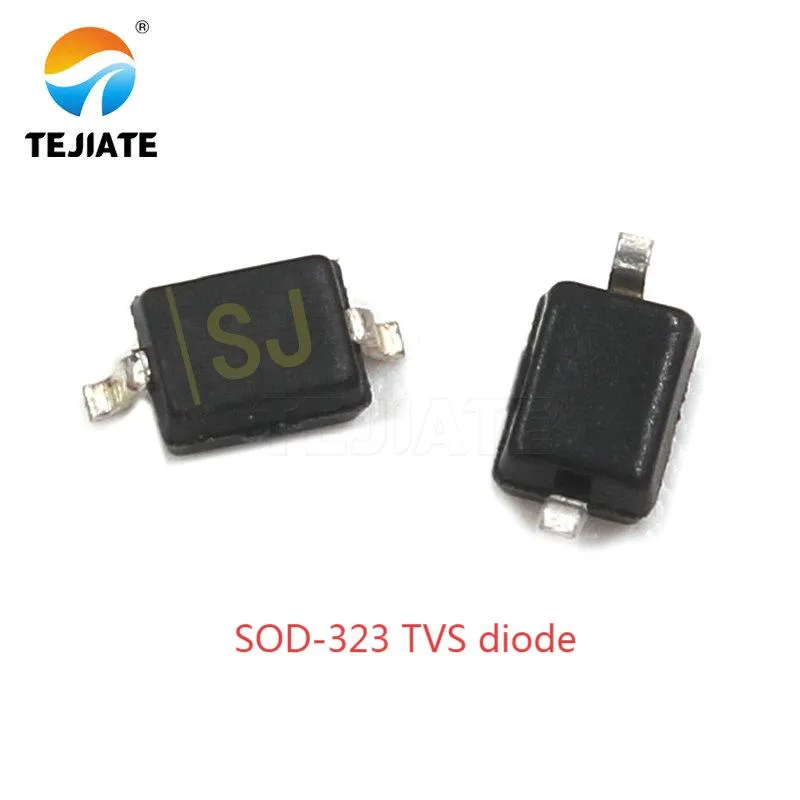
This image serves to establish a basic impression of the TVS diode, likely showing the device's physical appearance or symbol, emphasizing its "bodyguard" role in the circuit, and introducing the importance of key parameters such as Working Reverse Voltage (VRWM), Breakdown Voltage (VBR), and Clamping Voltage (VC).
A Transient Voltage Suppressor (TVS) diode is the quiet bodyguard that stands between your circuit and every electrical storm. You rarely notice it—until a static discharge, lightning surge, or automotive load dump hits the line. Whether your board runs on 5 V, 12 V, or 24 V rails, the wrong diode can clamp too late or leak too early.
The key is balance. The working reverse voltage (VRWM) must sit just above the normal line voltage, the breakdown voltage (VBR) should trigger fast under transients, and the clamping voltage (VC) must stay safely below your load’s limit. A low junction capacitance (CJ) keeps high-speed or RF paths intact.
At TEJTE, engineers validate every SOD-323 TVS diode against real automotive conditions—VRWM 15 V / 24 V, VBR 17.1 V / 25.4 V, VC 44 V / 70 V, CJ 13 pF @ 1 MHz, Ipp 3 A (8/20 µs), and 160 W peak-pulse power. Each part meets AEC-Q automotive grade, RoHS3 environmental compliance, and MSL 1 moisture rating, ensuring long-term reliability on dense PCBs. This same design discipline carries through TEJTE’s RF connector installation and waterproofing practices, which follow the same 50-ohm grounding precision required for stable ESD protection.
How do I pick a TVS diode for 5 V / 12 V / 24 V rails?
Align VRWM to nominal voltage (incl. tolerance)
Selecting the right TVS diode starts with aligning its VRWM to the system’s nominal rail. For a 5 V logic rail, choose a part with VRWM ≈ 5 V (±5%) so it stays reverse-biased under normal operation. A 12 V automotive line typically rises to 14.4 V during charging, meaning a VRWM ≥ 14 V part is safer. For a 24 V industrial bus that can momentarily reach 28 V, select VRWM ≥ 26 V.
A simple engineering rule:
VRWM ≈ 1.05 × V_nom (for regulated rails)
VRWM ≈ 1.2 × V_nom (for unregulated rails)
Following this keeps leakage low while avoiding false conduction during transient spikes. Such alignment also helps maintain transient voltage suppressor diode response integrity—critical for equipment that must meet IEC 61000-4-2 ESD protection levels.
Margining between VBR and VC under real pulses
Once VRWM fits the rail, compare VBR (min) and VC (max) under rated surge. For example, TEJTE’s 24 V SOD-323 TVS diode has VBR = 25.4 V and VC = 70 V at 3 A (8/20 µs). That gives a 45 V clamping margin, easily within IEC 61000-4-2 Level 4 (±8 kV contact) limits.
The check formula is:
Clamp Margin = Load Max Voltage − VC (max)
If your device tolerates 80 V, margin = 10 V — safe. If it fails at 50 V, the clamping voltage is too high.
Engineers often run this quick estimation when comparing data sheets or when migrating from a general ESD protection diode to an automotive-grade transient voltage suppressor.
Selection Matrix – 5 V / 12 V / 24 V Comparison
| Line Voltage | VRWM (V) | VBR (min V) | vC (max V @ Ipp) | Ipp (8/20 μs) | CJ (pF @ 1 MHz) | Package | PPP (W) | Uni/Bi | IEC 61000-4-2 Level | AEC-Q | RoHS3 | MSL |
|---|---|---|---|---|---|---|---|---|---|---|---|---|
| 5 V Logic | 5.0 | 6.4 | 9.2 | 30 A | 400 | SOD-323 | 13 | Uni | Level 4 (±8 kV) | 1 | Yes | 3 |
| 12 V Auto | 15 | 17.1 | 44 | 3 A | 160 | SOD-323 | 13 | Bi | Level 4 (±8 kV) | 1 | Yes | 3 |
| 24 V Bus | 24 | 25.4 | 70 | 3 A | 160 | SOD-323 | 13 | Bi | Level 4 (±8 kV) | 1 | Yes | 3 |
Approximate power validation:
PPP ≥ Ipp² × R_load × PulseWidth
Designers can use this matrix to benchmark tvs diode 5 v 8.5 v options or compare low-capacitance models for high-speed data lines. For advanced layout tips, review TEJTE’s WiFi Antenna Guide: 433 MHz, 4G, 5G, GSM & SMA Types, which discusses how impedance and capacitance interact in multi-GHz environments.
Bidirectional vs Unidirectional: When is bi-directional mandatory?
USB / Differential, CAN/LIN, Automotive I/Os
Reverse battery and inductive kick scenarios
When the circuit faces reverse polarity or coil flyback, a unidirectional TVS diode works better. It blocks in the normal direction and clamps only positive transients, ideal for relay or motor outputs on 24 V buses. The 44 V – 70 V clamp range of TEJTE’s device covers most inductive kicks without excess leakage.
For broader coordination between protection elements, the design approach follows TEJTE’s Automotive Fuse/TVS Co-Design principles explained in this reference blog.
Will 13 pF, 40 pF, or < 1 pF kill my signal?
Impact on RF / high-speed (VSWR / eye diagram)

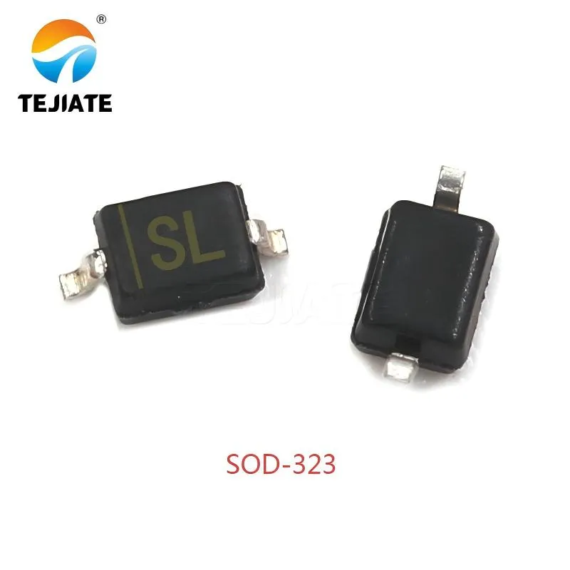
This image serves as a reference for the compact SOD-323 package, aiding designers in PCB layout and soldering. It emphasizes how this package is suitable for dense PCBs and is associated with TEJTE device's automotive-grade (AEC-Q), RoHS3, and MSL 1 reliability qualifications.
Capacitance is the hidden enemy of high-speed integrity. Even a 13 pF TVS diode adds roughly 245 Ω of reactance at 50 MHz, which may be fine for CAN or LIN buses but disastrous for RF or USB 3.0 lines. Once frequency climbs past hundreds of MHz, excess capacitance reflects energy back toward the driver, increasing VSWR and distorting the eye pattern.
That’s why engineers specify low-capacitance TVS diodes (< 1 pF) for RF front ends or differential pairs. TEJTE’s SOD-323 automotive TVS diode already maintains a modest 13 pF @ 1 MHz, making it suitable for signal lines below 10 MHz, yet it should be replaced by sub-pF types for antenna or HDMI ports.
Real-world lab tests show that when replacing a 40 pF suppressor with a 1 pF device, insertion loss improves by > 1.5 dB at 2.4 GHz, and eye-height degradation nearly disappears.
To better understand how impedance mismatches behave across frequency, TEJTE’s WiFi Antenna Guide offers practical insight into VSWR behavior on 2.4/5/6 GHz links and reinforces why signal integrity depends on capacitance as much as connector precision.
Quick bandwidth estimate: fc ≈ 1 / (2π · 50 Ω · CJ)
For a rough idea of when a transient voltage suppressor diode starts loading the signal, use
fc ≈ 1 / (2π · 50 Ω · CJ).
A 13 pF device yields ~245 MHz cut-off; 1 pF stretches it beyond 3 GHz. This heuristic helps decide whether your ESD protection diode should remain near the connector or be relocated deeper into the PCB trace where impedance control is looser.
Where exactly should I place the TVS on the PCB?
Near connector, shortest return path, lowest loop inductance
Placement is the real determinant of ESD performance. A perfectly specified TVS diode fails if it sits a centimeter away from the connector. Every millimeter of trace adds inductance—about 1 nH/mm—which can translate into 1 V of overshoot per A of transient current.
Always mount the TVS as close as physically possible to the interface pin. Route its cathode directly to the line and its anode to a low-impedance ground plane using the widest via pair available. Keep the return loop compact and symmetric for differential ports.
The same grounding principles appear in TEJTE’s RF Connector Installation, Cleaning & Waterproofing, where mechanical sealing and electrical grounding are co-optimized to maintain 50-Ω continuity under surge and vibration.
Partitioning for multi-port products
In devices with multiple interfaces—say, Ethernet + USB + CAN—avoid grouping all TVS diodes in a single cluster. Each port should have its own local return path and ground stitching via. Separate copper zones prevent mutual coupling during IEC 61000-4-2 ESD events.
High-density designs may require creative stacking: an array package near USB, discrete diodes near automotive connectors. This approach keeps parasitic loops minimal and improves repeatability during surge certification.
How to test a TVS diode with a DMM and an oscilloscope?
Static checks: open / short / leakage
Testing a TVS diode starts simple. With power removed, measure resistance both directions using a multimeter’s diode mode. A healthy device reads open in reverse and around 0.6–0.8 V forward (for unidirectional types). Infinite resistance both ways suggests an open failure; near-zero in both indicates a short.
For bidirectional TVS diodes, expect symmetrical forward drops around ±0.7 V. To assess leakage, switch to the mega-ohm range—good parts typically exceed 10 MΩ under VRWM.
Field technicians often perform this test after ESD events; it’s fast, non-destructive, and catches most failures before they propagate into downstream ICs.
Dynamic checks: ESD gun / conducted surge & clamp waveform

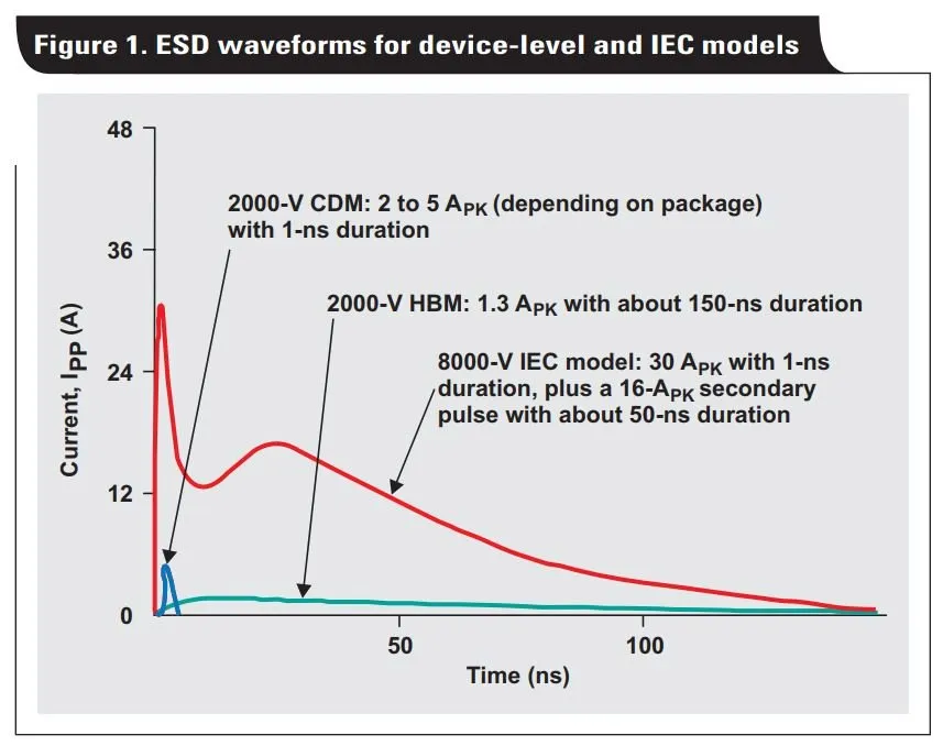
This chart is key to understanding and verifying the dynamic performance of TVS diodes. It visually presents typical current waveforms under 2000V CDM, 2000V HBM, and 8000V IEC models (peak current, pulse duration), helping engineers set correct test conditions and interpret the captured clamping waveforms on an oscilloscope, ensuring the device meets requirements like IEC 61000-4-2 Level 4 (±8kV contact discharge).
For true validation, you’ll need an oscilloscope and an ESD gun or surge generator following IEC 61000-4-2 or -4-5 waveforms. Connect the probe across the protected node, fire an 8 kV contact discharge, and capture the voltage peak.
A well-designed transient voltage suppressor like TEJTE’s SOD-323 series should clamp around its specified VC (44 V or 70 V) and recover within tens of nanoseconds. If the waveform shows excessive overshoot or long tail recovery, review placement and grounding before blaming the diode.
For layout examples that illustrate both surge and RF integrity, see TEJTE’s RF Cable Loss Analysis at 2.4/5/6 GHz; its discussion on coax attenuation directly parallels the energy dissipation principles behind TVS testing.
Automotive & compliance: AEC-Q, RoHS3, REACH, MSL explained
Why AEC-Q & MSL1 matter in OEM / aftermarket
When qualifying an automotive TVS diode, data-sheet numbers aren’t enough. OEMs demand AEC-Q101 qualification—thermal cycling, humidity bias, and pulse life testing—to ensure survival through 1,000+ surge cycles. TEJTE’s SOD-323 transient voltage suppressors meet this grade, combining AEC-Q validation with MSL 1 moisture sensitivity, which means they can be reflowed repeatedly without dry-bake requirements.
For design engineers working in both OEM and aftermarket domains, AEC-Q and MSL are not just labels—they’re survival criteria. Parts installed near engine control modules face temperature swings from –65 °C to +150 °C, along with mechanical vibration. Failure of an ESD protection diode in this zone can cause sensor resets or data-line instability. Choosing compliant devices reduces warranty exposure and guarantees predictable clamping behavior across lifetime stress.

This image highlights a key qualification for automotive-grade TVS diodes. AEC-Q101 certification means the device has undergone rigorous thermal cycling, humidity bias, and pulse life testing, ensuring survival through 1000+ surge cycles in harsh automotive environments including temperature swings from -65°C to +150°C and mechanical vibration, which is crucial for both OEM and aftermarket applications.
BOM and documentation tips

This image is likely a flowchart or breakdown diagram used to illustrate how to determine the ECCN for an electronic component (like a TVS diode). It probably shows the five-character structure of an ECCN (e.g., category, product group, control reason), explains the classification process, and emphasizes the importance of correct classification for export control compliance.

This image exemplifies the key document or identification proving that a TVS diode or other electronic component is classified as EAR99. The EAR99 category means the item is not controlled under a specific ECCN but is still subject to the general provisions of the EAR. Such proof documents (potentially from the supplier or through self-classification) are crucial for product export, customs clearance, and providing compliance assurance to customers and distributors, forming an essential part of the BOM and export documentation package.
Regulatory documentation must always mirror the product’s declared conformity. Each TVS diode in your bill of materials should carry clear references to RoHS3, REACH, and AEC-Q101 compliance. For internal records, maintain the supplier’s environmental declaration (like TEJTE’s SGS certification from 2022) alongside the data sheet revision.
When exporting assemblies, customs often require proof of ECCN EAR99 classification, confirming the device’s non-restricted status. These compliance details are small but crucial when your product enters regulated markets.
For designers integrating both RF and power-transient elements, review TEJTE’s N-Type Connector Outdoor Install & IP67 Sealing Guide — it highlights how environmental resilience and electrical robustness overlap in every 50-Ω interface.
Field mistakes to avoid
Under-spec’d VRWM / VC, power curve misuse
A classic error is choosing a TVS diode with VRWM slightly below nominal voltage—perhaps to “improve response.” In reality, this forces leakage, heating, and premature degradation. Always allow at least 5–10% voltage headroom. Another frequent oversight: misreading the pulse power (PPP) curve. The 160 W rating for TEJTE’s SOD-323 model applies to an 8/20 µs pulse, not continuous load. Doubling pulse width halves power handling.
Similarly, mismatched VC selection can overstress the protected IC. If your microcontroller tolerates 30 V, pick a diode clamping below 25 V—not a 44 V version meant for 12 V rails. Real protection is about matching dynamic response, not chasing the highest rating.
High-C device on RF / high-speed ports; poor placement
Another trap: using a high-capacitance transient voltage suppressor diode (like 40 pF) directly on a 2.4 GHz or HDMI line. It will reflect and attenuate signals, often failing EMC tests. Always pick low-capacitance TVS diodes (< 1 pF) for RF ports and place them within a few millimeters of the connector.
When evaluating ESD failures, engineers often find the TVS too far from the contact point, or routed through thin traces that added 10–15 nH of inductance. As discussed in TEJTE’s RF Connector Cleaning & Grounding Practices, short and wide return paths are just as critical for surge control as for RF continuity.
FAQ — TVS Diode Selection & Testing
Q1. How do I choose VRWM and VC for a 12 V automotive rail?
Pick a TVS diode with VRWM ≥ 14 V and VC ≤ 44 V under 3 A (8/20 µs). That ensures it stays off at nominal voltage but clamps hard during surges. Verify that VC lies below the ECU’s absolute maximum input.
Q2. When should I use a bidirectional TVS instead of a unidirectional one?
Use bidirectional TVS diodes for AC-coupled or differential lines (USB D+/D-, CAN H/L, LIN). They protect both polarities symmetrically without distorting the waveform.
Q3. Will a 13 pF TVS diode degrade my RF or high-speed signal, and how can I estimate the risk?
At 50 Ω, the –3 dB cutoff for 13 pF is ~245 MHz. Above that, expect reflection and insertion loss. For RF or multi-GHz buses, switch to low-capacitance TVS diodes (< 1 pF).
Q4. What’s the simplest multimeter check to spot an open or shorted TVS diode?
Measure both directions: open in reverse, ~0.6–0.8 V forward for unidirectional parts. Shorts read near 0 Ω, opens show infinite.
Q5. How do I place the TVS near a connector to minimize loop inductance?
Keep the TVS diode physically next to the interface pad, with a short, wide trace to ground. Avoid daisy-chaining protection devices.
Q6. Does a TVS diode protect against reverse battery connection, or do I still need polarity protection?
No. A transient voltage suppressor only clamps overvoltage spikes; it does not block DC reverse polarity. Add a series diode or MOSFET for full polarity protection.
Q7. What documentation should I keep for AEC-Q, RoHS3, REACH, and MSL compliance?
Keep the supplier’s conformity certificates (like TEJTE’s SGS RoHS3 and REACH reports) in your BOM folder and reference them in project documentation to simplify audits.
Final Note
Bonfon Office Building, Longgang District, Shenzhen City, Guangdong Province, China

A China-based OEM/ODM RF communications supplier
Table of Contents
Owning your OEM/ODM/Private Label for Electronic Devices andComponents is now easier than ever.
