MOSFETs: BUK7K6R8-40E,115 40V Dual N Guide
Oct 27,2025
Preface

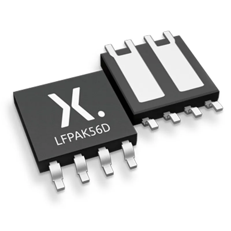
The image likely shows a typical application block diagram, product appearance, or placement on a circuit board for this MOSFET, aiming to establish an initial impression of this 40V, AEC-Q101 qualified device utilizing TrenchMOS™ technology.
In 12 V and 24 V power designs, the MOSFET you pick quietly decides more than just current flow—it shapes thermal headroom, reliability, and long-term efficiency. Engineers who’ve burned through prototypes know that Rds(on), Qg, and thermal resistance often matter more than headline voltage ratings.
This article centers on BUK7K6R8-40E,115, a 40 V dual N-channel TrenchMOS™ part that’s AEC-Q101 qualified and rated up to 175 °C. With key parameters—Id = 40 A, Rds(on) ≈ 6.8 mΩ @ Vgs = 10 V, Qg ≈ 28.9 nC, and Ciss ≈ 1947 pF—it offers a mix of high current density and manageable switching charge.
We’ll translate those numbers into real design behavior: what this means for 12 V or 24 V buses, which gate drivers match best, and how PCB layout affects watt-level efficiency.
Should you use a dual N-channel 40 V MOSFET for 12/24 V loads?
For most embedded power stages, the answer is yes—if transient control is well handled.
A 40 V MOSFET gives a comfortable 60–70 % voltage margin over a 24 V rail, which is enough when your surge and ESD protections follow IEC 61000-4-2 guidelines. Designers often clamp transient peaks below 38 V using a TVS diode or snubber network, keeping the device safely within its Vdss = 40 V window.
Below is a quick load-to-design map used in many 12 V/24 V systems:
| Load Type | Typical Supply | Peak Current | Design Note |
|---|---|---|---|
| 12 V motor | 12-14 V | 20-25 A | Keep ~50 % SOA margin with a TVS diode |
| 24 V heater | 24-28 V | 15-20 A | Prioritize low Rds(on) and heavy copper pours |
| LED or PWM driver | 12 V | 5-10 A | Qg < 30 nC helps lower EMI |
| Relay coil / solenoid | 24 V | 3-5 A | Always add flyback suppression |
How does BUK7K6R8-40E,115 fit your design window?

This image is the official product photo or typical appearance illustration of this specific MOSFET model, aiding engineers in visual identification during component selection, procurement, and PCB layout. It visually presents the device's markings, pin orientation, and overall form factor in the LFPAK56D package, serving as a direct visual reference to the parameter table below it.
| Parameter | Typical Value | Practical Insight |
|---|---|---|
| Vdss | 40 V | Safe for 12/24 V rails with 30-40 % surge margin |
| Id (25 °C) | 40 A | Each channel supports > 20 A continuous with copper plane |
| Rds(on) | 6.8 mΩ @ Vgs = 10 V | Minimizes heat in high-duty PWM loops |
| Qg (max) | 28.9 nC @ 10 V | Allows < 1 A driver for sub-100 ns edges |
| Ciss / Coss / Crss | 1947 / 220 / 90 pF | Predictable dv/dt behavior |
| Vgs(th) | 4 V @ 1 mA | Logic-level compatible; ideal for 5-10 V drivers |
| RθJA / RθJC | 62 °C/W / 2 °C/W | Solid heat spreading on 4 cm² copper |
| Tj (max) | 175 °C | Wide thermal margin for automotive modules |
| Qualification | AEC-Q101 | Ensures consistent automotive reliability |
With Pmax = 64 W, it fits mid-range DC-DC converters, LED drivers, and motor controllers.
You can estimate conduction losses by:
[ P_{cond} = I^2 \times R_{ds(on)} \times D ]
At 20 A and 50 % duty, (P_{cond} ≈ 2.7 W) per channel—manageable with standard copper pours. Switching losses add proportionally with frequency, which we’ll calculate in later sections.
Pick N-channel vs P-channel: which topology wins here?
In low-voltage power electronics, N-channel MOSFETs dominate because their electron mobility yields roughly one-third the Rds(on) of similar P-channels. For 12 V and 24 V rails, that difference directly translates into cooler devices and higher system efficiency.
Trade-off summary:
- Low-side switching — simplest and most efficient; gate tied to ground reference, ideal for heaters or pumps.
- High-side switching — isolates load from supply but needs a bootstrap or charge-pump driver raising gate ≈ 8–10 V above Vbus.
- Half-bridge designs — one high-side + one low-side FET; dual packages like BUK7K6R8-40E,115 ensure symmetrical parasitics and timing.
At Vgs = 10 V, the part’s 6.8 mΩ Rds(on) keeps efficiency above 95 % even under heavy load. Designers migrating from discrete singles often note 15–20 % lower junction temperatures due to tighter thermal coupling.
Which gate-driver strategy should you adopt?

This schematic explains how to select the appropriate driving strategy based on the MOSFET's position in the circuit (low-side, high-side, or half-bridge). It may include the gate driver IC, bootstrap capacitor, diode, and key waveforms, emphasizing the need for crisp, well-controlled gate drives for devices with Qg ≈ 28.9 nC to optimize switching performance, reduce EMI, and minimize losses.
Driving a dual N-channel MOSFET like the BUK7K6R8-40E,115 looks simple on paper, but in practice, gate behavior defines both efficiency and noise. The gate-driver topology depends on where your MOSFET sits—low-side, high-side, or half-bridge.
For low-side switching, the choice is straightforward. Logic-level drivers that output 5–10 V can directly control the MOSFET because the Vgs(th) is around 4 V. With Qg ≈ 28.9 nC, a small gate driver supplying 0.5–1.0 A peak is enough to achieve sub-100 ns transitions at typical PWM frequencies (100–500 kHz).
When you move to high-side configurations, you’ll need a bootstrap driver or an isolated driver IC. The bootstrap capacitor should charge during the low-side conduction period and lift the gate voltage about 8–10 V above Vbus during switching. A rule of thumb:
[ C_{boot} \ge 10 \times Q_g / \Delta V ]
For Qg = 28.9 nC and ΔV = 1 V, you’d select Cboot ≈ 300 nF—standard for 200–400 kHz buck converters.
Dead-time control is equally crucial. Too little, and both MOSFETs conduct simultaneously; too much, and body diode losses rise. A 200–500 ns dead-time is a good starting point for 12 V or 24 V synchronous converters.
In summary, low Rds(on) parts like the BUK7K6R8-40E,115 benefit from crisp, well-controlled gate drives rather than brute-force current. Clean transitions minimize EMI, reduce switching loss, and protect the gate oxide during IEC 61000-4-2 level ESD events.
How do you budget MOSFET power dissipation honestly?
1. Conduction Loss
[ P_{cond} = I^2 \times R_{ds(on)} \times D ]
At 20 A, Rds(on) = 6.8 mΩ, and 50% duty, the conduction loss is about 2.72 W per channel. Temperature rise affects this too—Rds(on) can increase by 50% when junction temperature climbs from 25 °C to 125 °C.
2. Switching Loss
[ P_{sw} \approx 0.5 \times V \times I \times (t_r + t_f) \times f_s + Q_g \times V_{gs} \times f_s ]
Assume V = 24 V, I = 20 A, tr + tf = 80 ns, fs = 200 kHz, and Qg = 28.9 nC. You’ll see Psw ≈ 1.8 W. Combining both gives Ptotal ≈ 4.5 W per FET under continuous operation.
3. Junction Temperature Rise
[ \Delta T_j = P_{total} \times R_{\theta JA} ]
With RθJA ≈ 62 °C/W, junction rise reaches ~280 °C theoretically—but that’s worst case. In real layouts with 4 cm² copper and airflow, effective thermal resistance drops near 25–30 °C/W, keeping ΔTj ≈ 120 °C.
In field practice, designers often derate total power by 30% to cover driver losses, body diode conduction, and PCB heating. Thermal vias, thicker copper, and grounded thermal pads can reduce temperature by another 10–15 °C.
If your PCB carries both power and signal lines, maintain short return paths. TEJTE’s post on IP67 connector sealing and grounding covers how grounding continuity can also help thermal spreading in outdoor or high-current environments.
By combining datasheet equations with realistic derating, you avoid the trap of “datasheet optimism” and get results that match the bench within ±10%.
Can layout alone save several watts?

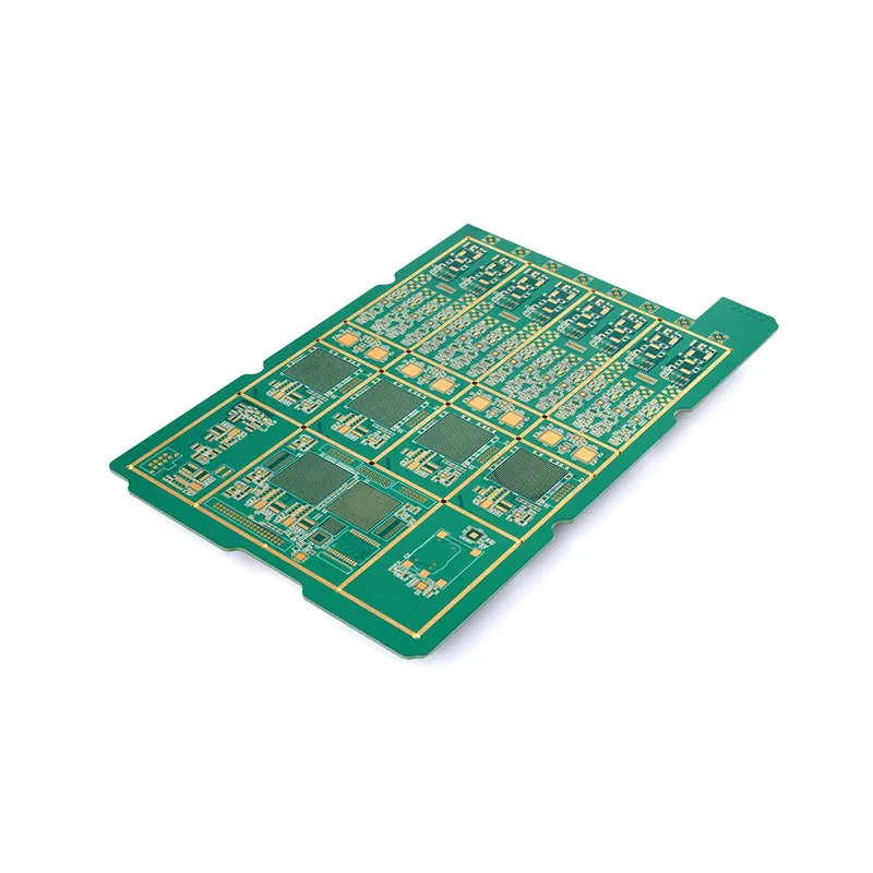
This schematic specifically demonstrates how careful layout can reduce power dissipation and improve thermal management. It likely includes symmetrical Drain/Source copper planes to ensure current balance between the two channels, a gate driver loop kept under 10mm, RC snubbers (e.g., 100Ω+1nF) placed close to the pins, and 3-4 thermal vias under the LFPAK56D package pads – measures that collectively can save several watts of loss.
Absolutely. Even with perfect parts, poor layout can waste more power than component losses. A dual N-channel MOSFET like BUK7K6R8-40E,115 depends heavily on symmetry and copper geometry.
1. Paralleling rules:
When using both channels in parallel, ensure the drain and source copper planes are equal in width and length. Uneven trace resistance makes one FET carry more current, heating unevenly. Ideally, keep both drain paths under 5 mΩ difference.
2. Ground and driver routing:
The gate-driver loop must be short—less than 10 mm from driver output to gate pin and back to source. Adding a 2–5 Ω gate resistor per channel can balance switching and damp oscillation.
3. Snubbers and EMI control:
Compact RC snubbers (e.g., 100 Ω + 1 nF) across drain–source terminals absorb voltage spikes from wiring inductance. Place them as close as possible to pins to prevent ringing.
4. Thermal optimization:
For LFPAK56D packages, add at least 3–4 thermal vias under each tab. Each via can lower local thermal resistance by ~5 °C/W. Combined with thicker copper (2 oz), total temperature reduction often exceeds 10 °C.
When carefully optimized, a clean PCB layout can save 2–3 W of dissipation in a 24 V, 20 A loop—sometimes more than the gain from changing to a pricier FET.
In short, layout is your passive heatsink. Each millimeter of copper, each trace bend, and every via impacts thermal balance, EMI, and lifetime reliability. Get that right, and even a compact 40 V MOSFET pair runs comfortably below 125 °C junction at full load.
What changed in IEC 61000-4-2 (2025) and why should you care?

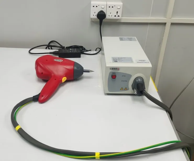
This image likely depicts an ESD test configuration compliant with the new standard requirements, including a calibrated discharge gun, reference planes, and protection measures for the MOSFET gate, such as gate clamp diodes, RC filters, or transient absorbers (TVS), ensuring gate-source voltage stress remains within the ±20V safe window even during ±8kV contact discharge events.
The upcoming IEC 61000-4-2 Edition 3.0 (2025) refreshes how engineers must verify ESD robustness in power electronics. While this standard traditionally covered electrostatic discharge for data and communication ports, it now extends calibration and test requirements for power switching paths—including MOSFET gates and their immediate periphery.
The main updates include:
- Calibration tightening — pulse current waveform tolerances reduced from ±15 % to ±10 %.
- Test setup standardization — mandatory reference planes and updated rise-time requirements for air and contact discharge guns.
- Measurement repeatability — stricter energy delivery verification at 8 kV and 15 kV, reflecting real field discharge events.
- Expanded test coverage — explicit testing of gate-source and drain-source pins in high-impedance states.
In short, this version no longer treats ESD as a signal-integrity problem alone. Power designers are expected to validate ESD resilience at component level, not just at connector interfaces.
For MOSFET-based systems, it means verifying that your gate clamp diodes, RC filters, or transient absorbers keep gate oxide stress under ±20 V even during ±8 kV contact discharges. The BUK7K6R8-40E,115, built on TrenchMOS™ technology and tested for AEC-Q101, already meets much of this expectation—but the board around it must too.
TEJTE’s post on TVS diode selection and ESD protection networks expands on the coordination between MOSFET gates and surge clamps under this updated IEC framework.
If you validate hardware to IEC 61000-4-2 Ed. 3.0, always document waveform shape, coupling method, and clamp voltages. Certification labs such as HV Technologies and EMC Partner already apply these updated procedures, so aligning your test plan early saves re-testing costs later.
Where is the market headed—and how does it impact sourcing?
The automotive and industrial MOSFET market is moving fast toward compact dual packages and trench designs. Between 2025 and 2033, analysts project a compound annual growth rate (CAGR) above 7 % for automotive-grade N-channel MOSFETs, driven by EV subsystems, ADAS modules, and 48 V power rails.
For purchasing and design engineers, that growth carries three key implications:
- Supply tightness for 40 V trench devices. Many vendors, including Nexperia, Infineon, and ROHM, have shifted capacity to 80–100 V lines for EV traction inverters. That makes efficient 40 V dual parts like the BUK7K6R8-40E,115 strategically valuable for 12/24 V domains.
- Quality differentiation. Tags such as AEC-Q101, 175 °C rating, and trench cell geometry have become practical quality flags rather than marketing lines. These parameters signal silicon robustness, die density, and packaging maturity—all of which matter in supply-chain risk reviews.
- Regional sourcing shifts. Post-2025 trade policies encourage more local sourcing for automotive semiconductors. Distributors like Digi-Key and Mouser now highlight origin and wafer-fab location for automotive customers under new labeling rules.
When shortlisting suppliers, prioritize those offering full lot-traceability, packaging transparency, and consistent thermal-impedance data. TEJTE’s broader insights on RF connector manufacturing quality and traceability are equally relevant here—supply consistency directly affects long-term device reliability.
Build your shortlist now
| Model | Package | Vdss | Id (25 °C) | Rds(on) @ Vgs, Id | Qg @ Vgs | Ciss / Coss / Crss | SOA Note | RθJA | AEC-Q101 | Use Case (motor/LED/heater) | Driver Hint |
|---|---|---|---|---|---|---|---|---|---|---|---|
| BUK7K6R8-40E,115 | LFPAK56D | 40 V | 40 A | 6.8 mΩ @ 10 V | 28.9 nC | 1947 / 220 / 90 pF | Balanced dual | 62 °C/W | Yes | Heater, LED, motor | Logic-level 5-10 V |
| IRF7749L2 (Infineon) | PQFN 5×6 | 40 V | 35 A | 7.5 mΩ @ 10 V | 30 nC | 2100 / 240 / 100 pF | SOA limited >25 A | 70 °C/W | Yes | DC buck / relay | Bootstrap required |
| AON6424 (Alpha & Omega) | DFN 8×8 | 40 V | 50 A | 5.5 mΩ @ 10 V | 32 nC | 1900 / 200 / 80 pF | High thermal eff. | 50 °C/W | NO | Motor / LED driver | Logic driver or isolated |
You can quickly approximate loss and temperature rise during early design using these equations:
[ P_{cond} = I^2 \times R_{ds(on)} \times D ]
[ P_{sw} \approx 0.5 \times V \times I \times (t_r + t_f) \times f_s + Q_g \times V_{gs} \times f_s ]
[ \Delta T_j = (P_{cond} + P_{sw}) \times R_{\theta JA} ]
Example:
For I = 20 A, Rds(on) = 6.8 mΩ, V = 24 V, tr+tf = 80 ns, fs = 200 kHz, and RθJA = 62 °C/W, total junction rise ≈ 120 °C.
If you halve switching frequency or improve copper spreading, temperature drops by 20–25 °C—demonstrating how layout and driver tuning directly translate to reliability.
Frequently Asked Questions (FAQ)
1. Is a 40 V MOSFET enough for a 24 V motor with voltage spikes?
Usually yes—provided that your design includes proper surge and ESD suppression.
A 40 V MOSFET such as BUK7K6R8-40E,115 offers roughly 30–40 % voltage margin above a 24 V rail.
Use a TVS diode rated between 33–36 V, or include an RC snubber to keep transients under the device’s Vdss = 40 V limit.
When testing under IEC 61000-4-2 (2025), make sure that gate voltage never exceeds ±20 V relative to source—even during contact discharge events.
2. When does a dual N-channel package outperform two single devices?
Dual packages like LFPAK56D reduce trace length and heat-spreading imbalance.
Because both dies share the same copper slug, their junction temperatures remain nearly identical, improving thermal symmetry and EMI behavior.
In synchronous buck or half-bridge stages, this balance cuts conduction and transition mismatch, often improving efficiency by 2–3 % compared with discrete FETs.
3. How should I size a gate driver for a 6–10 mΩ MOSFET?
Start from the total Qg—in this case ≈ 28.9 nC @ 10 V.
A good heuristic is to source 5–10× Qg per switching cycle, so a driver capable of 0.5–1 A peak easily handles 200–500 kHz switching.
If your topology includes a high-side FET, add a bootstrap capacitor roughly 10 × Qg / ΔV (≈ 300 nF).
Avoid over-driving beyond 10 V Vgs, which only increases EMI and ringing without lowering Rds(on) further.
4. What dead-time is safe for a synchronous buck running at 200–500 kHz?
Typical safe values range between 200 ns and 500 ns, depending on diode reverse-recovery time and driver delay.
Too little dead-time causes shoot-through current; too much increases body-diode conduction loss.
Always confirm using an oscilloscope—observe drain-source voltage overlap and ensure current flow reverses smoothly before the complementary FET turns on.
5. Does “TrenchMOS™” automatically mean lower switching loss?
Not always.
TrenchMOS™ technology reduces Rds(on) dramatically, but switching loss still depends on Coss, Crss, and Qg.
Compare the ratio of Coss : Crss—a small value (≈ 2–3 × difference) indicates faster charge removal and less stored energy.
For high-frequency converters, always check the Qg × Vgs × fs term in your total loss equation to get the full picture.
6. What changed in IEC 61000-4-2 Edition 3.0 (2025)?
Edition 3.0 introduces tighter calibration limits, standardized reference planes, and mandatory energy-verification steps at 8 kV / 15 kV.
For designers, it means you must verify ESD protection directly at the MOSFET gate, not just at connector level.
Your test log should include waveform traces, clamp voltage, and discharge current values to comply with the new reporting requirements.
Labs such as HV Technologies and EMC Partner have already adopted these updates in their certification workflow.
7. Is BUK7K6R8-40E,115 suitable for automotive 12 V rails?
Yes.
It’s AEC-Q101 qualified, rated to 175 °C, and optimized for 40 A continuous drain current.
This makes it ideal for fans, relays, thermal heaters, and other 12 V load switches.
Just ensure that PCB copper area supports at least 3–4 thermal vias and that gate drive stays within the ±20 V safe window during transient events.
Final Takeaway
The BUK7K6R8-40E,115 proves how modern TrenchMOS™ dual N-channel technology can simplify 12 V / 24 V platforms without compromising safety or efficiency.
By respecting updated IEC 61000-4-2 (2025) requirements, using a realistic power-loss model, and treating PCB copper as an active thermal component, engineers can achieve near-laboratory reliability even in compact housings.
For extended reading on grounding and low-loss routing principles that complement MOSFET design, TEJTE’s detailed post on RF cabling and outdoor routing ties together the electrical, mechanical, and EMC perspectives every designer eventually faces.
Bonfon Office Building, Longgang District, Shenzhen City, Guangdong Province, China

A China-based OEM/ODM RF communications supplier
Table of Contents
Owning your OEM/ODM/Private Label for Electronic Devices andComponents is now easier than ever.
