SMA Connector PCB Layout: Tips for 50Ω Launch & Routing
Oct 4,2025
The image highlights how minor changes—pad oversizing, missing via fences, or tight clearances—can detune 50Ω impedance, causing return loss spikes above 2 GHz.
Designing an RF board is always a balancing act. On the CAD screen, the traces look neat and predictable, but in practice the way you implement an sma connector pcb layout often determines whether the design performs flawlessly above 2 GHz or ends up failing during lab validation. A pad that’s slightly oversized, a ground clearance that’s too tight, or a missing via fence can shift impedance by just a few ohms. That small change is enough to cause reflections, bandwidth reduction, and, in the worst case, another costly board spin.
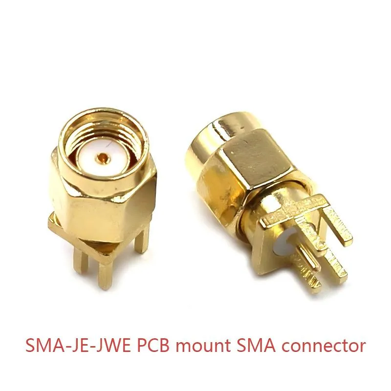
Over the years, our team has integrated thousands of SMA, SSMA, and MCX connectors into Wi-Fi routers, IoT gateways, and test equipment. Each project reinforces the same lesson: the connector launch is never “just mechanical.” For instance, the SMA-JE-JWE PCB mount SMA connector is rated 0–6 GHz, RoHS-compliant, with a brass gold-plated shell. Meanwhile, the SSMA-KE edge-launch type is smaller, designed for 50 Ω up to 3 GHz, and built with PTFE dielectric for stability. These real-world parts show how small mechanical choices directly shape RF behavior.
If you’ve ever held a board and wondered why the return loss spikes at 5 GHz despite a clean simulation, chances are the launch details are to blame. That’s why it helps to step through the main checkpoints—form factor, impedance control, transitions, and assembly—before the board goes to fab. Think of it as building insurance into your layout, instead of trying to fix things later with adapters or tuning stubs.
Identify your form factor: edge-mount, end-launch, or vertical?
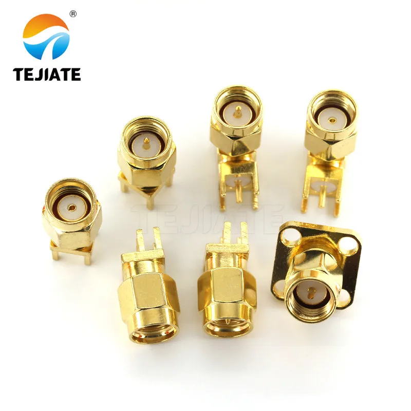
The image compares three SMA mounting families—edge-mount for compact side connections, end-launch for precision up to 12 GHz, and vertical for robust mechanical retention.
SMA connectors on PCBs usually fall into three families: edge-mount, end-launch, and vertical (through-hole). The differences are not just cosmetic—they affect both RF performance and ease of assembly.
- Edge-mount slides over the side of the board, with its center pin soldered directly to a top-layer trace.
- End-launch is more precise, often used in high-frequency test boards, sometimes up to 12 GHz.
- Vertical types use posts or legs that drop through the board, providing strong mechanical retention.
One quick visual check: the SMA-JE series shows 0.9 mm plated through-holes with a 6.5 mm square footprint, while SSMA edge-launch versions rely on side flanges and shorter tails. That small difference changes how the solder joint forms and how the launch behaves at high frequencies.
When to pick dedicated SMA PCB connectors
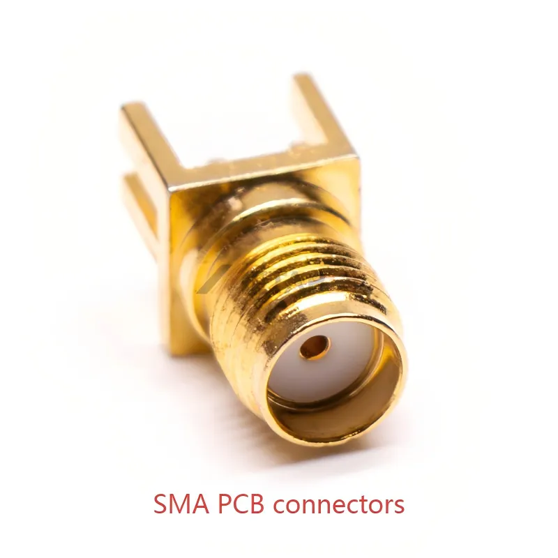
The image shows the SMA-JE-JWE footprint (1.6 mm leg spacing, 0.9 mm drill) designed for VSWR ≤ 1.20 @ 6 GHz, avoiding mismatches common in generic libraries.
It can be tempting to drop in a generic SMA footprint and call it done. In reality, that shortcut usually leads to mismatches. With high-speed designs, even slight misalignment between pad size and connector pin geometry shows up as poor return loss. A dedicated pcb mount sma connector avoids those issues by matching datasheet geometry.
For example, the SMA-JE-JWE footprint specifies a 1.6 mm leg spacing and guarantees a VSWR better than 1.20 through 6 GHz. These details rarely exist in generic libraries, but they make the difference between a clean launch and a troubleshooting nightmare. Matching datasheet values with your PCB stackup is the simplest way to ensure repeatable, reliable performance.
Hit 50 Ω on the first spin: how to size traces?
Microstrip/stripline calculator
This figure provides key design parameters (e.g., hole size, pad diameter, leg pitch) essential for precise PCB layout, 50-ohm impedance control, and via fence placement. The table and formulas below the figure further explain how to calculate microstrip trace width based on the PCB stackup to achieve the target impedance.
| Parameter | Symbol | Value | Notes |
|---|---|---|---|
| Dielectric constant | εr | 4.2 | FR-4 datasheet |
| Substrate thickness | h | 0.8 mm | Core to ground |
| Copper thickness | t | 35 μm | Standard 1 oz copper |
| Target impedance | ZO | 50 Ω | SMA system |
| Calculated width | W | ≈1.5 mm | For microstrip |
Formula reference:
Z0 ≈ (60 / √εeff) · ln(8h/W + W/4h)
εeff ≈ (εr+1)/2 + (εr−1)/2·(1/√(1+12h/W))
At 2.4 GHz, placing a via fence every ~3 mm (λg/20) produces a noticeably cleaner launch. In our own builds using the SMA-JE straight-leg footprint, tightening the via pitch reduced reflection peaks that previously showed up in S11 sweeps.
Bends and arcs for SMA connector PCB trace routing
Routing is where things get messy. A 90° corner looks tidy on CAD, but RF signals don’t like it. At 2.4 GHz, the penalty might be minor. At 5.8 GHz, you’ll often see measurable discontinuities.
Two safer approaches:
- 45° chamfers: easy to draw, and they trim down excess capacitance at corners.
- Curved arcs: even better for broadband launches, especially above 6 GHz.
In one TEJTE board with an SMA-JE-JWE pcb sma connector footprint, switching from a sharp 90° trace to a smooth arc lowered the local impedance bump by nearly 2 Ω. That tiny tweak translated into visibly cleaner TDR results—something you appreciate when your spectrum plot finally looks flat.
Optimize the launch transition to reduce return loss
Pads, anti-pads, keep-outs, and ground openings
The connector launch is more than a piece of metal soldered onto the board—it’s part of the RF path. Get it wrong, and your nice flat impedance turns into a rollercoaster.
- Pad size: follow the datasheet closely. For example, the SMA-JE-JWE specifies a 0.9 mm drill with a 1.7 mm pad. Oversizing the pad increases capacitance.
- Anti-pad clearance: open the ground plane around the pin by at least two to three times the drill diameter. Too small and you add stray capacitance; too large and inductance creeps in.
- Keep-out: keep copper pours away from the launch region. Stray metal under the center pin can distort impedance.
- Taper: don’t jump straight from a fat pad to a narrow line—ease the transition.
In our lab tests with SMA-JE parts rated up to 6 GHz, reducing the anti-pad size caused VSWR to spike above 1.25 at 5 GHz. Restoring the clearance smoothed out the S11 curve immediately.
Use MIL-STD-348A and footprint libraries wisely
The U.S. MIL-STD-348A standard defines the mechanical interface for SMA connectors. While you may not need full military precision, referencing it helps avoid surprises in your sma connector pcb layout.
EDA libraries in Altium or Eagle often include a pcb sma connector footprint, but don’t assume it’s perfect. One client reused a generic SMA footprint with 5.08 mm leg spacing. Unfortunately, the actual TEJTE SMA-JE required 6.5 mm. The result? Pins didn’t line up, solder joints were off-center, and performance dropped. A quick check against the datasheet could have prevented a week of rework.
Fence the ground: where and how many vias?
Edge-mount via arrays and spacing to metalwork
In any sma connector pcb layout, the launch won’t perform well unless the ground return is tightly controlled. That’s why RF designers almost always use a via fence around the trace.
For an sma pcb edge mount connector, a few simple rules go a long way:
- Place the first via as close as physically possible to the pad.
- Keep via-to-via spacing around λg/20—roughly 3 mm at 2.4 GHz in FR-4.
- Stick to hole sizes that match your stackup, typically 0.3–0.5 mm drills.
We validated this with the SMA-JE straight-leg connector (0–6 GHz). Boards with sparse fences showed sharp S11 peaks above 5 GHz. After adding more vias along each side, the return loss curve flattened back into spec.
Pro tip: don’t wait until full RF testing to verify your fence. Even a continuity check with a simple ohmmeter will tell you if all vias are well tied into ground.
Bulkhead/panel tie-ins for mechanical robustness
Vias aren’t just for RF. They also share the mechanical load of the connector shell. When a bulkhead SMA is fastened to a front panel, torque often transfers straight into the PCB. By stitching vias around the mounting pads, you spread that stress across the board instead of letting a single joint take the hit.
In one IoT gateway build, missing vias near the launch caused the solder tails to crack after only 200 mating cycles. Once we added a proper fence tied to the ground plane, durability jumped back above the 500-cycle rating listed in the datasheet.
Choose straight vs right-angle without killing bandwidth
Detuning risks and mitigations
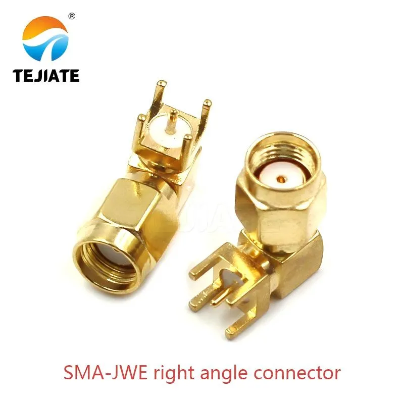
This figure illustrates the right-angle connector solution used when enclosure space is limited. The document context notes that right-angle versions introduce extra parasitic inductance and capacitance compared to straight types, potentially limiting usable bandwidth and requiring compensatory design in the ground plane and via stitching.
A straight connector is the cleanest option electrically, but real-world enclosures don’t always allow it. That’s when designers reach for a sma right angle connector. The trade-off? Extra parasitic capacitance and inductance that can shrink usable bandwidth.
In our own testing, the SMA-JE-JWE straight connector held VSWR under 1.20 all the way to 6 GHz. The right-angle version, by contrast, drifted up to 1.25 around 5 GHz. On paper that may seem minor, but in a narrow-band filter or a high-Q circuit, that difference shows up as degraded performance.
To offset these effects:
- Open up the ground plane slightly beneath the elbow to ease capacitance.
- Add reinforced via stitching around the bend to keep the return path tight.
- Keep the trace between the launch and first bend as short as possible.
Consider a short SMA extension cable instead
If mechanical clearance is the problem, a straight launch plus a short jumper is often the safer bet. A SMA extension cable from the board to the panel avoids the parasitics of a hard right-angle mount.
Advantages:
- Preserves bandwidth up to 6 GHz.
- Adds flexibility during assembly and maintenance.
Drawbacks:
- Introduces one more connector interface, with insertion loss of roughly 0.1–0.2 dB at 6 GHz (based on TEJTE’s lab data).
For prototypes, the flexibility usually outweighs the loss. In high-volume production, you’ll need to weigh assembly efficiency against RF margin. Either way, thinking through these trade-offs early in your sma connector pcb layout saves surprises later.
Solder or reflow without failing pull tests
Soldering/reflow spec card
| Process | Spec | Notes |
|---|---|---|
| Reflow | Peak 245 °C, 30-60 s above 217 °C | Follow JEDEC profile strictly |
| Hand solder | 350-370 °C, ≤3s contact | Longer contact risks PTFE damage |
| Flux | ROLO or RMA, no-clean preferred | Reduces post-cleaning steps |
| Cleaning | IPA if residue visible | Avoid flooding the connector body |
| Pull force | ≥0.28 N (center pin), ≥45 N shell | Matches TEJTE datasheet specs |
AQL sampling and visual criteria
A robust QC plan doesn’t end at one perfect sample. For how to solder sma connector to pcb, inspectors typically apply AQL sampling (e.g., 1% of each lot) and reject parts that show:
- Lifted or cracked pads.
- Cold joints with dull or grainy surfaces.
- Flux residue bridging the shell and the pin.
- Cracks after torque or durability tests.
In practice, when the SMA-JE-JWE was soldered within profile, it passed more than 500 mating cycles without issue—consistent with datasheet claims. By contrast, rushed hand-solder jobs with overheated flux often failed pull testing before 200 cycles. The difference wasn’t the connector, but the process.
Should I choose female or male, and how does it mate with other connectors?
Pairing with SMA male/female and adapters
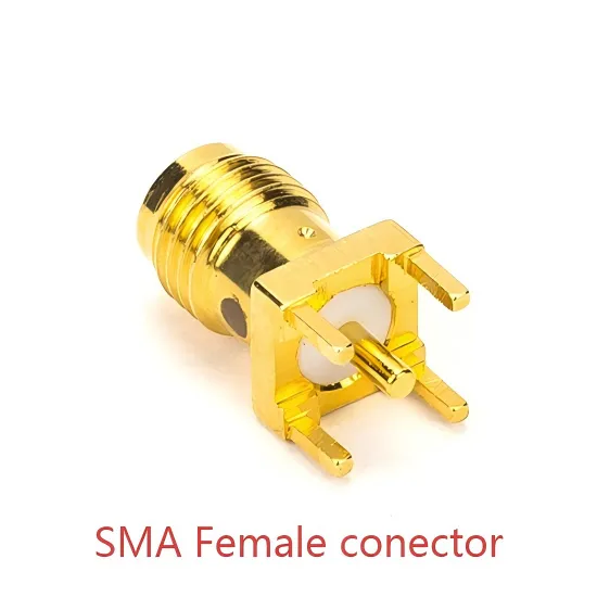
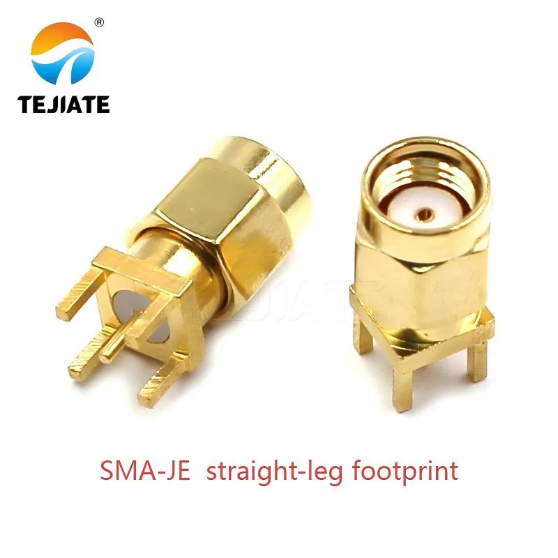
This figure depicts the most common type of onboard SMA connector. The document explains that female connectors are typically used on PCBs to mate with standard male test cables, antennas, etc., forming the fundamental interface for device interconnection and testing.
Connector gender is more than a mechanical label—it defines how the PCB connects with the rest of your RF chain. Most boards use an sma female connector, since antennas, test cables, and many lab instruments terminate in male plugs. The SMA-JE series from TEJTE, for instance, offers inner-thread female sockets rated from 0–6 GHz with VSWR ≤1.20, a safe match for both prototypes and production runs.
There are times, though, when an sma male connector on the board makes more sense—especially if it mates directly with a female bulkhead in the enclosure. To bridge between test setups, you’ll often rely on an sma adapter, or even an sma to bnc adapter when dealing with legacy oscilloscopes. Each adapter adds a small insertion loss (around 0.1–0.2 dB @ 6 GHz), so it’s smart to keep the adapter chain short.
Field tip: before heading into the lab, check that your team actually has the right adapter. More than once, we’ve seen testing delayed simply because an sma to bnc adapter wasn’t on hand.
Using 50 Ω SMA cables and crimps for board extensions
When the RF signal must leave the board, short jumpers become essential. The most reliable option is a sma cable assembly using 50 ohm coax cable, terminated with a sma crimp connector. This setup maintains impedance control while adding mechanical flexibility.
In one IoT build, switching from a rigid right-angle mount to a 10 cm sma cable assembly improved the return loss curve and reduced solder joint stress. It’s a small change, but it paid off in both performance and durability.
What files do I need to submit before ordering?
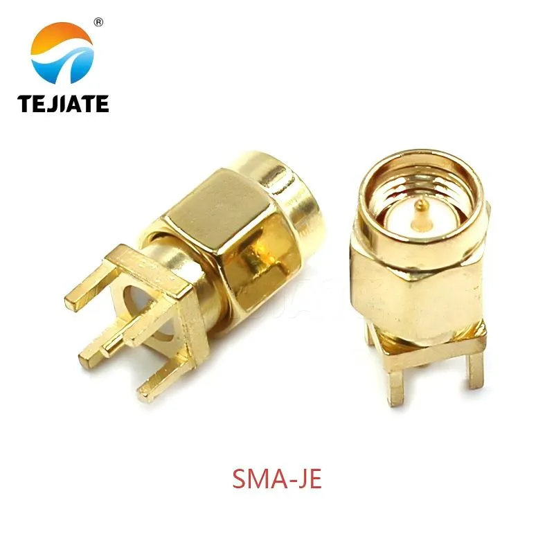
This figure is a critical reference for final design and procurement, providing precise overall dimensions of the connector, such as shell size, mounting hole locations, and overall height. These dimensions are vital for PCB layout, stencil design, and enclosure cutouts, ensuring the connector installs and mates correctly.
Suppliers can only deliver what you clearly specify. For an sma connector pcb layout, a proper data pack saves endless back-and-forth later. At a minimum, include:
- Gerber or ODB++ files with copper keep-outs, anti-pads, and via fences marked.
- Assembly drawings that highlight connector orientation and soldering details.
- Footprint tables with pad and hole dimensions. For example, the SMA-JE specifies a 0.9 mm drill, 6.5 mm square pad, and 1.6 mm leg pitch.
- Torque specifications for bulkhead or panel mounting (≈0.6 Nm typical).
- Compliance and traceability notes: RoHS status, cycle rating (≥500 insertions), and batch IDs.
In one telecom project, a team skipped torque data in the drawings. Installers overtightened the bulkhead nuts, cracking the PTFE dielectric. That mistake forced a costly redesign—proof that even “minor” details matter.
EDA resources and footprint control
A pcb sma connector footprint from Altium, Eagle, or KiCad is a good starting point, but never assume it’s exact. Cross-check with the connector’s datasheet before release.
At TEJTE, footprints are tied to specific part numbers and kept under version control. That prevents mix-ups like confusing PN 08772-09724 with PN 08357-08358—similar parts, but different leg spacing. Taking five minutes to confirm dimensions upfront avoids production headaches later.
Pro tip: always freeze connector footprints early in the design. Changing them late in the layout cycle often ripples through keep-outs, via fences, and panel cutouts, creating a chain of edits that delay release.
How do I run a 5-minute inspection after receiving samples?
IQC quick-check checklist
| Category | Check Item | Tool | Spec / Example |
|---|---|---|---|
| Visual | Plating quality, cracks | Loupe | Uniform gold, no voids |
| Dimensional | Footprint vs datasheet | Caliper | 0.9 mm drill, 6.5 mm pad |
| Mechanical | Durability cycles | Hand test | ≥500 cycles, no looseness |
| Torque | Thread fit / nut seating | Torque tool | ~0.6 Nm typical |
| Electrical | Continuity & insulation | Multimeter | ≥5000 MΩ, no shorts |
| RF quick | Return loss (S11) | Simple bridge | VSWR ≤1.20 @ 6 GHz |
Common issues to watch
Across projects, three failure patterns show up again and again in sma connector pcb layout reviews:
- Edge-mount misalignment: if the shell isn’t flush with the PCB edge, the launch detunes and reflections spike.
- Oversized ground windows: anti-pads opened too wide increase inductance instead of reducing capacitance.
- Sparse via fences: when spacing exceeds λg/20, resonant peaks emerge, especially near 5 GHz.
By catching these issues early, you can ensure the pcb sma connector footprint you designed in CAD actually works as intended in the real world.
How to run a 5-minute return loss and structure test?
Quick RF check with simple tools
Not every lab has a full VNA on hand. Even so, a handheld reflection bridge or compact analyzer can flag major problems in an sma connector pcb layout. Connect the board, sweep to 6 GHz, and look for two things:
- Return loss better than 20 dB (VSWR ≤1.20) across your operating band.
- No sudden spikes at 2.4 or 5.8 GHz, which often point to missing via fences or oversized anti-pads.
In one test with the SMA-JE-JWE pcb sma connector footprint, a properly sized anti-pad kept the S11 curve smooth through 6 GHz. A second build, with clearance cut too tight, showed a 15 dB dip near 5.5 GHz—an avoidable mistake.
Structural and mechanical spot checks
Even if you don’t run RF sweeps right away, basic mechanical checks reveal a lot:
- Verify solder wetting ≥90% around each pin.
- Apply at least 0.28 N pull on the center conductor to confirm strength.
- Torque the bulkhead nut to ~0.6 Nm and ensure the PCB doesn’t flex or crack.
FAQs
How wide should my top-layer trace be for a 50-ohm SMA launch on FR-4?
With FR-4 (εr≈4.2, h≈0.8 mm, 1 oz copper), the width is around 1.5 mm. Always calculate based on your actual stackup.
Do I really need a via fence, and how close should the vias be?
Yes, for GHz launches. Place vias at ~λg/20 pitch (~3 mm at 2.4 GHz). Wider gaps allow parasitic resonances.
What anti-pad size minimizes return-loss spikes at 2.4 and 5.8 GHz?
Clear ground at least 2–3× the drill diameter around the center pin. This reduces extra capacitance.
When should I pick a right-angle SMA instead of an edge-launch?
Only when enclosure height demands it. Otherwise, a straight connector with a short jumper cable is electrically cleaner.
Can I route across a split ground near the SMA pad?
No. Routing across splits detunes the launch and often creates resonances in S11 plots.
Is a short SMA jumper better than a right-angle for clearance?
Often yes. A jumper preserves bandwidth up to 6 GHz, while right-angles add parasitics.
What quick tests confirm my PCB launch is in spec?
Visual check, continuity/insulation test, torque verification, and a fast return-loss sweep.
Conclusion
A reliable sma connector pcb layout is rarely about one big decision—it’s the accumulation of many small, careful choices. The type of connector you mount, the way you size traces for 50 Ω, the spacing of via fences, and even the soldering profile all add up to determine whether your RF design works smoothly or struggles with reflections and losses.
The good news is that most of the common pitfalls are easy to avoid if you plan ahead. Stick closely to datasheet footprints, reference standards like MIL-STD-348A, and verify geometry before release. Adding quick inspections—like a five-minute IQC checklist or a return-loss sweep—catches most problems before they ever leave the lab.
It’s also worth remembering that the RF path doesn’t end at the connector. Using a properly matched 50 ohm coax cable or a short sma cable assembly ensures that the clean launch you designed on the PCB continues into the rest of the system. Many engineers overlook this handoff, only to discover performance drops once the board is integrated into real hardware.
For teams building Wi-Fi routers, IoT gateways, or telecom gear, the lesson is simple: SMA launches are not “just connectors.” They’re the handshake between your PCB and the outside world. Get them right, and everything downstream—antennas, cables, instruments—has a far better chance of working exactly as you intended.
Bonfon Office Building, Longgang District, Shenzhen City, Guangdong Province, China

A China-based OEM/ODM RF communications supplier
Table of Contents
Owning your OEM/ODM/Private Label for Electronic Devices andComponents is now easier than ever.
